† Corresponding author. E-mail:
Project supported by the National Science and Technology Major Project, China (Grant No. 2013ZX02308-002) and the National Natural Science Foundation of China (Grant Nos. 11435010, 61474086, and 61404099).
A novel groove-type channel enhancement-mode AlGaN/GaN MIS high electron mobility transistor (GTCE-HEMT) with a combined polar and nonpolar AlGaN/GaN heterostucture is presented. The device simulation shows a threshold voltage of 1.24 V, peak transconductance of 182 mS/mm, and subthreshold slope of 85 mV/dec, which are obtained by adjusting the device parameters. Interestingly, it is possible to control the threshold voltage accurately without precisely controlling the etching depth in fabrication by adopting this structure. Besides, the breakdown voltage (VB) is significantly increased by 78% in comparison with the value of the conventional MIS-HEMT. Moreover, the fabrication process of the novel device is entirely compatible with that of the conventional depletion-mode (D-mode) polar AlGaN/GaN HEMT. It presents a promising way to realize the switch application and the E/D-mode logic circuits.
GaN-based electronic devices have attracted more and more attention due to their excellent material properties such as high saturation electron velocities and breakdown electric fields.[1,2] Most of the reported AlGaN/GaN high electron mobility transistors (HEMTs) show D-mode operation because the two-dimensional electron gas (2DEG) exists at the heterointerface at a gate bias voltage of 0 V.[3] However, E-mode operation is essential for the safe operation of power electronic applications and the realization of various monolithic integrated enhancement-/depletion-mode (E/D-mode) digital circuits.
So far, several techniques for achieving the enhancement-mode (E-mode) operation in the AlGaN/GaN HEMTs have been reported, such as gate recess, fluoride-based plasma treatment, reducing the composition or the thickness of the AlGaN barrier, and a nonpolar a-plane channel. However, in the above techniques some problems still exist. Gate-recess is a viable approach;[4] but the threshold voltage cannot be easily reproduced by the dry etching technique, because the polarization charge density is highly dependent on the recess depth.[5] Another approach to fluoride-based plasma treatment may degenerate the device uniformity and make the devices very unstable.[6,7] As a part of the epitaxial design, the decreasing of the composition or the thickness of the AlGaN[8,9] to reduce the sheet charge can achieve the E-mode operation, but the increase of parasitic resistance between the source and the drain is difficult to overcome. As the above technique difficulties all arise from the purpose of reducing two-dimensional electron gas (2DEG) under the gate in polar AlGaN/GaN, the nonpolar AlGaN/GaN HEMT that is free from the polarization-induced sheet charges has attracted attention and been demonstrated with E-mode operation in recent years.[10–12] Some techniques such as Si δ-doping,[13] regrown n+-GaN contact layer,[14] and Al2O3 gate dielectric[15] have been adopted to improve the performance of nonpolar GaN-based HEMT. However, its maximum transconductance and maximum current density are still low compared with E-mode AlGaN/GaN HEMT on c-plane GaN. Thus, combining the advantages of the polar and nonpolar heterostructure to realize E-mode operation is expected to be a promising method to solve this problem. However, to the best of our knowledge, both the design and the fabrication of structure based on this concept have not been discussed so far.
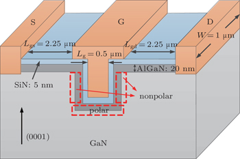
In this paper, a novel device structure called groove-type channel enhancement-mode AlGaN/GaN MIS HEMT (GTCE-HEMT) is presented, in which the recess etching and regrowth technology are adopted to realize the combination of the polar and nonpolar AlGaN/GaN heterostructure. These technologies are widely used in the fabrication process,[16–18] especially in the fabrication of the vertical GaN HEMT.[19–21] Therefore, the fabrication process of the GTCE-HEMT is compatible with that of the conventional D-mode devices. In this paper, we analyze the physical mechanism of the GTCE-HEMT to realize E-mode operation, and the influence of gate recess depth on the direct current (DC) characteristics, and then we investigate the mechanism of the GTCE-HEMT to improve the breakdown voltage by two-dimensional (2D) numerical simulations. The simulations show excellent device performances. Interestingly, by using the groove channel, the breakdown voltage (VB) is successfully increased compared with that of the conventional MIS-HEMT. Moreover, the Vth has a saturation value as the recess depth is beyond 500 nm. That is to say, when the recess depth reaches about 500 nm, a continued process of recessing has almost no effect on Vth. Therefore, the GTCE-HEMT can avoid the difficulty in controlling the threshold voltage by dry etching technique and improve the threshold voltage uniformity. In addition, the fabrication process of the GTCE-HEMT is compatible with that of the conventional D-mode devices.
The GTCE-HEMT structure is proposed and schematically shown in Fig.
| Table 1. Required characteristic for designing the GTCE-HEMT. . |
The analysis of the GaN-based HEMT in this paper is performed by SILVOCAL-ATLAS software. The positive sheet charge with a density of 1×1013 cm−2 at the interface between polar AlGaN and GaN is used to model the positive polarization charge.[22] Meanwhile, the fixed sheet charge along the nonpolar plane heterointerface is designed to be zero. Acceptor traps with a density of 1×1015 cm−3 located at 0.5 eV below the conduction band edge are employed in the buffer layer to model the carbon atomic pollution during the growth.[25] The Shockley–Read–Hall (SRH) carrier recombination model, constant low field mobility model, field-dependent mobility model at high electric fields, and the impact ionization model are used in the simulation study.[26] The low field electron mobility is designed to be 900 cm2/V·s and 50 cm2/V·s in the polar GaN region and nonpolar GaN region (the GaN region near the nonpolar AlGaN/GaN interface),[10,11,23] respectively. The impact ionization for GaN is described as α0exp(−EC/E) with α0 = 2.9 × 10⁸/cm, and EC = 3.4 × 10⁷ V/cm. All the simulations are carried out at the room temperature of 300 K. Under these conditions, the DC characteristics of the GTCE-HEMT are simulated and analyzed.
Figure
The natural structure of the III–V nitrides is wurtzite, a noncentrosymmetrical structure with polar axis, namely the c axis. The centers of positive and negative charges do not coincide in the equilibrium lattice of the III–nitrides at zero strain, hence inducing the spontaneous polarization along the polar axis.[31,32] Furthermore, with an applied stress, the lattice deformation induces a separation of the centers of the positive and negative charges in the crystal, thus forming dipole moments, the accumulation of which leads to the polarization charges on the crystal surface. This additional polarization in strained III–nitrides crystal is called piezoelectric polarization.[31–33]
In the (0001) plane AlGaN/GaN heterostructures, the spontaneous polarization occurs along the [000
For the nonpolar AlGaN/GaN, the crystal orientation is perpendicular to the polar axis, hence it is not affected by the polarization effect. In the undoped nonpolar heterostructure, no 2DEG is formed at the interface. This characteristic can be used to realize the E-mode operation. However, recent reports show that the electron mobility of the nonpolar heterostructure is still very low. One possible reason for the low mobility is the rough interface of the nonpolar heterostructure. The root mean square surface roughness is 2.8 nm on a-plane AlGaN/GaN measured by an atomic force microscope, as reported by Chang et al.[37] It is much larger than the root mean square surface roughness of 0.3 nm on the (0001) plane heterostructures. Besides, many dislocations in the nonpolar material also affect the electron mobility. As Kuroda et al.[10] reported, the density of the threading dislocations in the a-plane GaN is more than 1010 cm−2, which is much higher than 109 cm−2 in the c-plane GaN. Therefore, controlling the growth process to substantially improve the quality of the nonpolar crystal will be an important work to improve the electron mobility. In this paper, we just use the nonpolar materials at the sidewalls of the groove channel, thus significantly reducing the drawbacks of the nonpolar heterostructures.
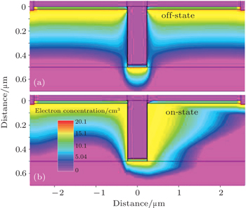
The 2DEG density and the energy band diagrams of the proposed GTCE-HEMT under different bias conditions are shown in Fig.
 | Fig. 3. Energy band diagram and electron density (a) underneath the gate region (polar AlGaN/GaN) and (b) on the sidewall of the groove (nonpolar AlGaN/GaN) with Vg = 0 V and 4 V at Vd = 0 V. |
The conduction band in the polar GaN region near the interface of the AlGaN/GaN heterostructure underneath the gate region is lower than the Fermi level EF even as no voltage is applied, which indicates the existence of 2DEG in the potential well as shown in Fig.
The gate recess depth is an important parameter in the ordinary gate-recessing HEMT, which affects the value of the threshold voltage, so discussion about the recess depth is necessary in this paper. Device models with various values of gate recess depth t are established to investigate the DC characteristics of the GTCE-HEMT with a gate metal work function of 5.2 eV. The thickness of SiNx and the nonpolar AlGaN are 5 nm and 15 nm, respectively. Figure
The DC characteristics of the devices with different recess depths can be explained by the short channel effect (SCE). As the channel at the bottom of the groove is always conductive under the normal switch condition, the sidewall of the groove channel near the source dominates the device characteristics. Thereby the effective gate length is actually the groove depth t, but not the horizontal gate length Lg. To mitigate the short-channel effects, the minimum aspect ratio (t/tbar) of 15 is proposed.[39] Herein, tbar = dAlGaN + dSiN. As tbar in this simulation is 20 nm, the recess depth should be larger than 300 nm. It means that short-channel effects such as the threshold voltage shift, transconductance decreasing, and the subthreshold slope deterioration may occur if the recess depth is lower than 300 nm. The conventional definition of the drain-induced barrier lowering (DIBL) (defined as ΔVth/ΔVd) is used to characterize the threshold voltage shift in HEMT. A plot of the simulated DIBL as a function of the recess depth is shown in Fig.
 | Fig. 6. Conduction band profiles along the channel of GTCE-HEMT for (a) 100 nm- and (b) 500-nm recess depth with different drain bias voltages. |
In order to further investigate the DIBL effect, the potential barriers of the channel with different drain bias voltages at Vg = 0 V are simulated and the results are shown in Fig.
In Fig.
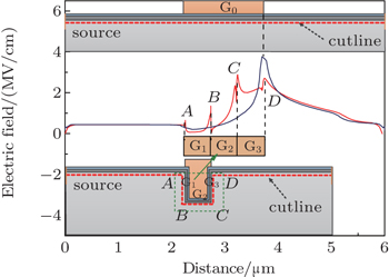
To further investigate the breakdown characteristic of the GTCE-HEMT, a conventional MIS-HEMT with a planar channel is simulated as a referential sample by using the same channel length and other device parameters as the GTCE-HEMT. The device simulation shows that GTCE-HEMT enhances the breakdown characteristics successfully by managing the electric field profile in the channel. The VB is significantly increased by 78% from 143 V of the conventional MIS-HEMT (recess depth of 0 nm) to 255 V of the GTCE-HEMT (recess depth of 500 nm).
 | Fig. 8. Electric field distributions along the interface of AlGaN/GaN for GTCE-HEMT (red line) and the conventional device (blue line). The dash line is from the source to the drain. |
The comparison in electric field distribution at the AlGaN/GaN interface between the 500-nm-recess depth GTCE-HEMT and the conventional MIS-HEMT is shown in Fig.
In this paper, we present a GTCE-HEMT that combines the polar and the nonpolar AlGaN/GaN heterostructure, and study its operation principle and DC characteristic by 2D simulations. A threshold voltage of 1.24 V, peak transconductance of 182 mS/mm, and subthreshold slope of 85 mV/dec are obtained by adjusting device parameters. Interestingly, a large variation of recess depth has almost no effect on the threshold voltage when the recess depth is up to 500 nm, which indicates a good tolerance of the etching process in the fabrication. In addition to this, by using the short channel effect, we also analyze the reason why the threshold voltage conspicuously shifts towards the negative direction as the recess depth is reduced to less than 300 nm. Moreover, the proposed structure is feasible to broaden the high-field region and hence reduce the peak electric field intensity, which makes breakdown voltage be 78% higher than VB of the conventional MIS-HEMT. In addition, as the fabrication process of GTCE-HEMT is compatible with that of the conventional D-mode devices, this structure can realize the possibility of achieving the switch application and the E/D-mode logic circuit.
| 1 | |
| 2 | |
| 3 | |
| 4 | |
| 5 | |
| 6 | |
| 7 | |
| 8 | |
| 9 | |
| 10 | |
| 11 | |
| 12 | |
| 13 | |
| 14 | |
| 15 | |
| 16 | |
| 17 | |
| 18 | |
| 19 | |
| 20 | |
| 21 | |
| 22 | |
| 23 | |
| 24 | |
| 25 | |
| 26 | |
| 27 | |
| 28 | |
| 29 | |
| 30 | |
| 31 | |
| 32 | |
| 33 | |
| 34 | |
| 35 | |
| 36 | |
| 37 | |
| 38 | |
| 39 | |
| 40 |


