


Electrical control of magnetism in oxides
[Song Cheng†,  , Cui Bin, Peng Jingjing, Mao Haijun, Pan Feng]
, Cui Bin, Peng Jingjing, Mao Haijun, Pan Feng]
|
|


† Corresponding author. E-mail:
Project supported by the National Natural Science Foundation of China (Grant Nos. 51322101, 51202125, and 51231004) and the National Hi-tech Research and Development Project of China (Grant Nos. 2014AA032904 and 2014AA032901).
Recent progress in the electrical control of magnetism in oxides, with profound physics and enormous potential applications, is reviewed and illustrated. In the first part, we provide a comprehensive summary of the electrical control of magnetism in the classic multiferroic heterostructures and clarify the various mechanisms lying behind them. The second part focuses on the novel technique of electric double layer gating for driving a significant electronic phase transition in magnetic oxides by a small voltage. In the third part, electric field applied on ordinary dielectric oxide is used to control the magnetic phenomenon originating from charge transfer and orbital reconstruction at the interface between dissimilar correlated oxides. At the end, we analyze the challenges in electrical control of magnetism in oxides, both the mechanisms and practical applications, which will inspire more in-depth research and advance the development in this field.
The electrical control of magnetism is an exciting new area of condensed-matter research with the potential to impact magnetic data storage, spintronics and high-frequency magnetic devices.[1,2] In paving its way toward spintronic-integrated circuits with ultralow power consumption, impressive improvements have been made to the properties of such nanoscale devices based on current-induced magnetization switching using spin-transfer torque (STT).[3,4] Further significant reductions in switching power by using an electric field are envisaged, reducing the energy dissipation by a factor of 100 when compared with that in STT devices, making it comparable to that in the present semiconductor field-effect transistors, but with added non-volatile functionality.[1,2]
The electrical control of magnetism is of interest not only because of its technological importance, but also because it allows us to uncover properties of magnetic materials that are otherwise inaccessible.[2] In 2000, the electrical control of the magnetic phase transition was first demonstrated in magnetic semiconductor (In,Mn)As,[5] which was used as a channel material in a field-effect transistor. Following the investigations on magnetic semiconductors, researchers began to explore the electrical control of ferromagnetic metals. It was previously assumed that a large electric-field effect in metals would be difficult to observe[6] owing to the associated short screening length, but the first observation of a direct electric-field effect on magnetism in a metal was reported for thin layers of FePt and FePd due to large electric-field-induced modulation of surface charges.[7] These successful studies encouraged more researchers to investigate the electrical control of magnetism in various systems, including the Fe(Co)/MgO[8,9] and CoFeB/MgO/CoFeB magnetic tunnel junctions (MTJs),[10,11] where the electrical control of magnetism is achieved by a change in interface magnetic anisotropy.
In the area of correlated complex oxides, the electrical control of magnetism has a much broader playground,[12] since in the complex oxide — which displays a variety of exotic properties such as ferromagnetic and superconductive two-dimension electronic gas — colossal magnetoresistance can be tuned by electrical methods. Furthermore, owing to the insulating or semiconductor nature of complex oxides, they often have much longer screening length, ensuring an electric field of sufficient strength for magnetic phase control.[13] On the other hand, the more recent developments have benefited greatly from the tremendous progress achieved in the past two decades in the controlled epitaxial growth of complex oxides, which has allowed the fabrication of ultrathin oxide films and heterostructures with atomic precision grown in controlled environments; the progress in the increasing variety of characterization tools dedicated to probing nanoscale phenomena; and the advances in first-principles calculation methods, which have enabled a deeper, atomic level understanding of the physical mechanisms underlying the strongly correlated behavior of metal oxides.[14] One of the exotic examples of electrical control of magnetism is in complex oxide multiferroics-based systems, where magnetoelectric (ME) coupling enables enhancing the magnetization switching induced by the application of electric fields.[2]
About the mechanisms involved in the electrical control of magnetism, there are a variety of answers. From the very beginning, the modulation of mobile carriers or surface charge by electrical control was considered to play a dominant role, especially in metallic magnetic materials[7,15] or diluted magnetic semiconductors (DMSs).[5,16] An induced or spontaneous electric polarization at the gate dielectric interface is screened by charge carriers from the channel layer, leading to charge accumulation or depletion and resulting magnetic properties. In the case of thin films of ferromagnetic semiconductors, this change in carrier density in turn affects the magnetic exchange interaction and magnetic anisotropy; in ferromagnetic metals, it instead changes the Fermi level position at the interface that governs the magnetic anisotropy of the metal.[2] Strain-mediated electrical control of magnetism is also a remarkable effect, especially in piezoelectric-based, ferroelectric-based[17,18] and multiferroics-based systems.[19] The external electric field alters the lattice or shape of the ferroelectric crystal by the converse piezoelectric effect during switching, and then transfers the strain to the proximate magnetic layer, leading to changes in magnetic anisotropy, magnetization rotation and coercion through the magnetostriction. Another novel mechanism to be mentioned is the oxygen migration effect or redox reaction effect especially at a metal-oxide interface or in oxide heterostructures, where the migration of oxygen causes a transition of ferromagnetic phase[20] or affects the orbital occupancy and magnetic anisotropy.[21]
The electric effect of magnetism is compatible with complementary metal–oxide–semiconductor (CMOS) technology and paves its way toward spintronic-integrated circuits with ultralow power consumption.[2] The motivation of our review is to provide a comprehensive summary of the rapidly developing area of electrical control of magnetisms and clarify their various mechanisms lying behind it. While much remains to be explored in terms of materials optimization, development and characterization, our review is aimed at illustrating how novel functionalities can be generated by exploring the new phenomena arising at the interface between dissimilar materials and how such an approach can be used to achieve more efficient electrical control of magnetism.
Multiferroic materials with the coexistence of ferroelectric (breaking of space inversion symmetry) and (anti-)ferromagnetic (breaking of time reversal symmetry) orders have drawn ever-increasing interest due to their magnetoelectric (ME) coupling effect and potential for applications in multifunctional devices.[22,23] However the rare single-phase multiferroic materials exhibit ME coupling at low Curie temperatures, and a high ME coupling above room temperature has not yet been found in the single-phase systems, limiting their practical application.[24–26] BiFeO3 (BFO) is unique, with high Curie and Néel temperatures far above room temperature, but it is G-type antiferromagnetic or only very weak ferromagnetic.[23]
The development of ME coupling is fortunately eased by the composite systems involving strong ferroelectric and ferromagnetic materials.[27,28] Greatly enhanced ME effect has been discovered experimentally in some two-phase nano-composites, such as BaTiO3–CoFe2O4,[29] PbTiO3–CoFe2O4[30] and BiFeO3–CoFe2O4.[31] The ME coefficient α in these composites is about three orders of magnitude higher than in those aforementioned single phase ME materials. A similar mechanism has also been explored in the ferromagnetic/ferroelectric heterostructures, whose physical images are unambiguous and design flexibilities are greater. Next we focus on these multiferroic heterostructures.
The electric field control of magnetic behavior has been realized by the ME coupling effect in a great number of multiferroic heterostructures: the classic ferroelectric (FE) crystal and films serve as the ferroelectric layer while the performance of (anti-)ferromagnetic metals, oxides, and diluted magnetic semiconductors (DMS) are modulated.[14,32] A detailed summary of the ME coupling constants, results of electric fields, and corresponding mechanisms in different systems are provided in Table
| Table 1. Summary of electrical control of magnetism in common multiferroic heterostructures. α is given in the unit of Oe·cm·V−1 (1 Oe = 79.5775 A·m−1), αr is the relative ME constant (dimensionless), and T is the temperature. The abbreviations are defined as follows: La1−xSrxMnO3 (LSMO), La1−xCaxMnO3 (LCMO), SrRuO3 (SRO), CoFe2O4 (CFO), BaTiO3 (BTO), Pb(Mg1/3Nb2/3)O3–PbTiO3 (PMN-PT), BiFeO3 (BFO), PbZr1−xTixO3 (PZT), PbTiO3 (PTO), YMnO3 (YMO), exchange bias (EB), magnetic anisotropy (MA), magnetization (M), Curie temperature (TC), coercivity (HC). . |
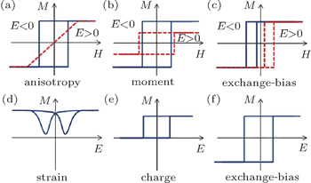
 | Fig. 1. Schematic of the different magnetic hysteresis curves expected in electrical control of magnetism (a)–(c) and the magnetoelectric coupling types in artificial multiferroics heterostructures (d)–(f).[14] |
Strain engineering is a powerful tool for manipulation of magnetism.[56–58] The strain-mediated electrical control of magnetism is considered to be the first attempt at designing an ME coupling in artificial FM/FE particulates and phase segregated ceramics,[59] and this approach has received renewed attention more recently.[60,61] This type of ME coupling was also widely reported in magnetic thin films (e.g. Ni, CoFeB, LSMO, and CFO) grown on ferroelectric substrates (e.g. BTO, PMN-PT, and PZT).[17,18,33–38,62–75] The external electric field alters the lattice or shape of the ferroelectric crystal by the converse piezoelectric effect, and then transfers the strain to the proximate magnetic layer, leading to changes in magnetic anisotropy, magnetization rotation, and coercivity through magnetostriction. In the FM/FE heterostructures, both (anti-)ferromagnetic oxides and metals are controlled by electric field.
In light of the rapid development of deposition technologies, such as oxide molecular beam epitaxy and reflection high-energy electron diffraction (RHEED)-assisted pulsed laser deposition (PLD), high-quality magnetic oxides can be epitaxially grown on ferroelectric substrates, constructing the cornerstone of electrical control of magnetism mediated by strain.[76] In 2007, Eerenstein et al. found a giant change in the magnetic moment of epitaxial 40-nm LSMO (x = 0.33) on single crystal BTO substrate with FE switching.[17] This variation in magnetization was attributed to the changes of magnetic anisotropy caused by strain coupling with non-180° BTO domain. The role of strain in this electrical manipulation was clearly demonstrated by Thiele et al. in the system of 20 nm–50 nm LSMO (x = 0.33) and LCMO (x = 0.33) on PMN-PT substrate.[18] The dependence of magnetization on electric field follows the relationship between in-plane piezoelectric strain and electric field in a butterfly shape, as shown in Fig.
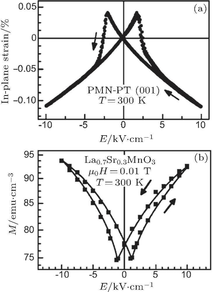 | Fig. 2. (a) In-plane piezoelectric strain versus applied electric field (E ∥ [001]) recorded along a [100] edge of a 0.72PMN–0.28PT substrate. (b) Magnetization M ∥ [100] versus E ∥ [001] applied to the substrate for an LSMO/PMN-PT (001) heterostructure.[18] |
Subsequently, strain-mediated electrical control of magnetism was observed in more and more oxide systems, with the realization of sharp and reversible changes in magnetization under electric field. Of course, the origins of strain-induced changes in magnetic properties have been vigorously pursued, with two mechanisms proposed to date: i) electrical control of electronic phase transition and ii) electrical modulation of magnetic anisotropy. The electronic phase transition driven by strain under electric field is supported by works using LSMO,[17,18] LCMO,[33] and Pr0.6Ca0.4MnO3[62] with a strong tendency toward phase separation in the ferromagnetic layer. In contrast, the changes of magnetic anisotropy under electric field was widely accepted in CoFe2O4[34,63] and Fe3O4,[35,36,64] where a magnetization orientation shift of 17° in Fe3O4/BaTiO3 was observed.[64]
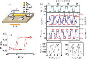
In addition to the successful epitaxial oxide-based ferromagnet, magnetic metal thin films, which are usually polycrystalline or amorphous, can also be tuned by electric field. The strain transferred from the substrate is proven to be able to alter the magnetic anisotropy of magnetic metal films. Compared with magnetic oxides, magnetic metal systems attract more attention due to their high TC, flexibility, and ease of production. The FE control of magnetic metal was observed in many systems like Fe/BTO,[65] Co/PMN-PT,[66,67] Ni/BTO,[38] CoFe/PMN-PT,[68] CoPd/PZT,[69] Fe-Ga/BTO,[70] CoFeB/PMN-PT.[71,72] The magnetic anisotropy, coercivity, magnetic moment, and magnetic switching were controlled by electric field in these systems. In a Co/PMN-PT heterostructure, both simulations and experiments demonstrated a macroscopically maneuverable and non-volatile 180° magnetization reversal at room temperature, as shown in Fig.
 | Fig. 3. (a) Pulsed electrical and magnetic operation and corresponding magnetic moments with a magnetic field of 3 Oe along [010] for Co/PMN-PT.[67] The different magnetization states are clarified as stage 1 (M ∥ [010]), stage 2 (M ∥    |
With the fast development of antiferromagnetic spintronics, more attempts are made in the control of antiferromagnetic materials by electrical means. Cherifi et al. used ferroelectricity in BaTiO3 crystals to tune the sharp metamagnetic transition temperature of epitaxially grown FeRh film and electrically drive a transition between AFM and FM order with only a few volts, just above room temperature [Figs.
In heterostructures where the magnetic properties are intimately linked to charge, a change in carrier doping level alters the magnetic performance. Two types of devices have been developed to realize the charge-mediated electrical control of magnetism: ferroelectric field effect transistors and multiferroic tunnel junctions.
The concept of field effect transistor (FET) could be taken as a reference here for designing artificial multiferroic structures to induce changes in the magnetic state. An induced or spontaneous electric polarization at the gate dielectric interface leads to charge accumulation or depletion and resulting magnetic property variations. For a ferroelectric material such as PZT, the charge carrier modulation is of the order of 1014 cm−2, which is much larger than that made possible by using silicon oxide as the dielectric gate.[77] More importantly, this effect is non-volatile after removing the electric field. The ferroelectric field effect transistor (FE-FET) has been used for a long time to modulate a variety of properties including superconductivity[78,79] and metal–insulator transitions.[80] In the past decade, the control of magnetism by FE-FET was reported, both in first-principles calculations and experiments, for a variety of systems, such as complex oxides, DMS, and metal ferromagnets.
In 2009, a dramatic magnetoelectric coupling mediated by the modulation of hole–carrier density was predicted in the La1−xAxMnO3/BTO (001) (A = Ca, Sr, or Ba) system by the first-principles method, where the doping concentration x was 0.5, near the FM–AFM phase transition.[81] The direction of BTO polarization was used to electrostatically manipulate the hole–carrier density in La0.5A0.5MnO3 and the resulting FM–AFM phase transition at the interface. When the polarization points away from (toward) the interface, there is an upward (downward) shift of the local density of states, favoring a hole charge accumulation (AFM) (depletion (FM)) state. Also, a microscopic model based on the two-orbital double exchange was introduced to describe this FE screening effect in manganites. The model simulation confirmed that the charge accumulation/depletion near the interface could drive the interfacial phase transition, which gives rise to a robust magnetoelectric response and bipolar resistive switching.[82]
The electric field control of magnetism mediated by charge modulation in FM oxide films was first observed by Molegraaf et al.[39] The magnetic response of PZT (250 nm)/LSMO (4 nm) as a function of applied electric field exhibits a magnetoelectric hysteresis curve, as reflected by the magneto-optic Kerr effect (MOKE) at 100 K in Fig.
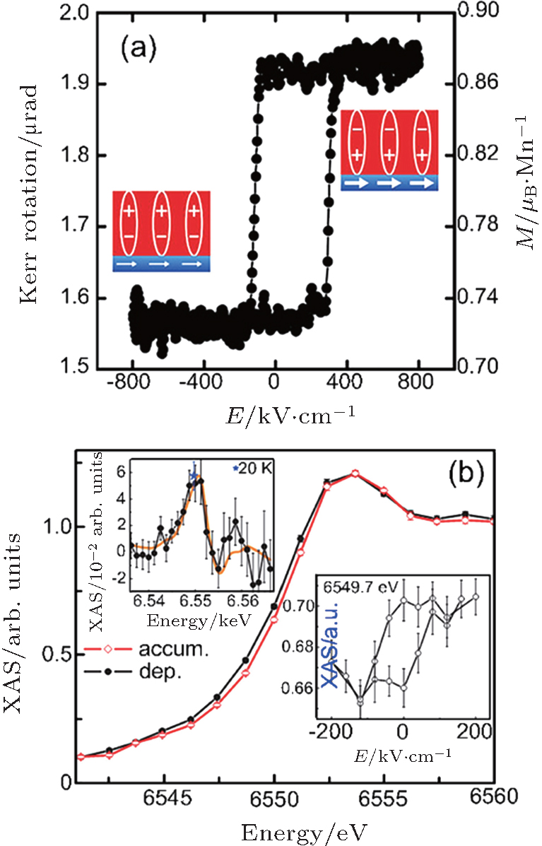 | Fig. 4. (a) Magnetoelectric hysteresis curve of the PZT/LSMO at 100 K.[39] (b) Room temperature XANES results for the two polarization states of the PZT. The left top inset shows the difference in x-ray absorption for the two PZT polarization states. The right bottom inset is the variation of the x-ray light absorption as a function of the applied gate voltage at a fixed energy, E = 6549.7 eV.[40] |
When we compare the strain- and charge-mediated cases, it is confusing that both the mechanisms of strain and carrier density appear in the same system, like in LSMO/BTO[17,84,85] and Fe/BTO.[47,48,65,87] It is noteworthy that modulation of carrier density induced by the electric field or polarization is mainly concentrated in the area near the interface, whose thickness is determined by the screening thickness (tS) of the FM layer:[6]

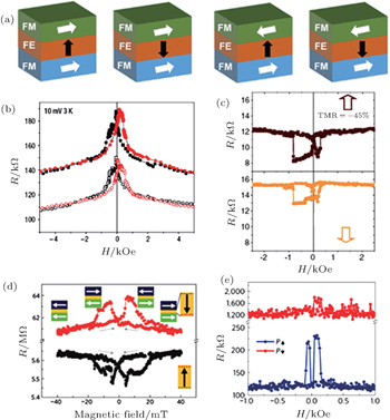
The electrical control of magnetism has also been realized in multiferroic tunnel junctions (MFTJs) where an FE (multiferroic) tunnel barrier is sandwiched between two FM (an FM and a normal metallic) electrodes.[92–98] The interaction between ferroelectricity and ferromagnetism can be studied through transport measurement, which displays four distinct resistance states due to the TMR and tunnel electroresistance (TER) effects, as shown in Fig.
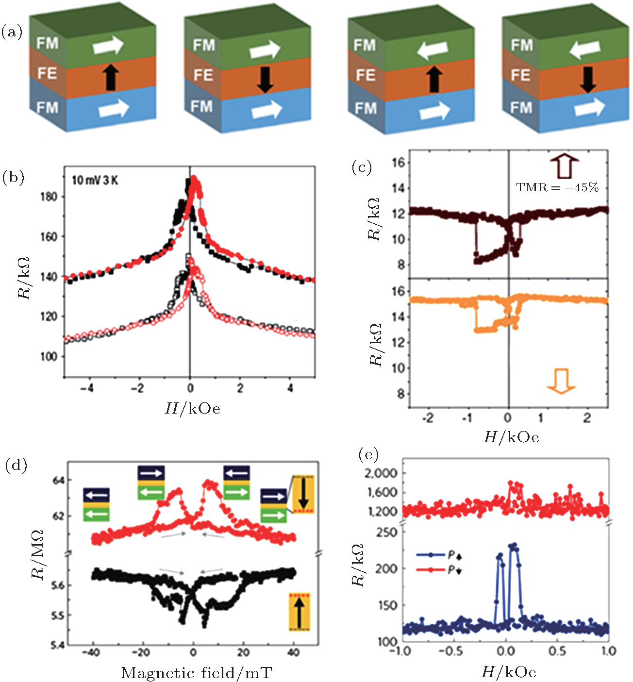 | Fig. 5. (a) Schematic diagram of the four resistance states in artificial MFTJS with two FM electrodes sandwiching an FE tunnel barrier. The white and black arrows represent the magnetic configurations and FE polarization, respectively. (b) Tunnel magnetoresistance curves at 4 K with Vdc. = 10 mV in an LSMO (x = 0.33)/LBMO(2 nm)/Au junction.[94] (c) Resistance versus magnetic field (R–H) curves for LSMO (x = 0.33)/BTO (1 nm)/Fe MFTJ (Vdc. = −50 mV, T = 4.2 K) after poling the ferroelectric barrier up or down, respectively.[95] (d) R–H curves measured at 50 K in the as-grown state of LSMO (x = 0.33)/PZT (3.2 nm)/Fe MFTJ.[96] (e) R–H curves for LSMO (x = 0.3)/LCMO (x = 0.5)/BTO/LSMO (x = 0.3) MFTJ.[97] |
The exchange bias effect is known to be associated with the coupling between FM and AFM materials, where the exchange coupling gives rise to a shift of the magnetic hysteresis loop away from the center of symmetry at zero magnetic field. When the single phase multiferroic materials like Cr2O3,[49–52] YMnO3,[53,99] LuMnO3,[100] and BiFeO3[19,54,55,101,102] (FE and AFM orders) serve as the FE layer, the exchange bias of heterostructure might be electrically reversed. The manipulation of exchange bias using intrinsic multiferroics allows the possibility of electric field switching of the direction of the magnetization.
Demonstration of exchange bias controlled by electric fields was first reported in perpendicularly magnetized [Co/(Pt or Pd)]/Cr2O3 heterostructures.[49–52] Reversible switching of the exchange bias was observed at 303 K in a [Co/Pd]/Cr2O3 (0001) heterostructure by simultaneous application of a magnetic field and an electric field to switch the antiferromagnetic single domain state, which in turn switched the direction of the uncompensated spins at the Cr2O3 (0001) interface that biased the [Co/Pd] hysteresis loop.[49] The electric field control of exchange bias in NiFe/YMnO3 was reported by Laukhin et al.,[53] who showed that the exchange bias, after cooling the system under a magnetic field, could be reduced to near zero by applying a voltage across the YMnO3.[99]
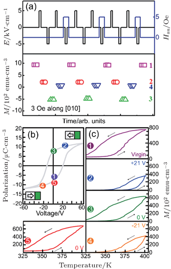
BFO is the most famous multiferroic materials with a ferroelectric TC of ∼ 1100 K and G-type AFM Néel temperature of ∼ 640 K.[24,103–106] The origin of exchange bias in G-type AFM BFO, with a fully compensated spin configuration at the interface, is related to the Dzyaloshinskii-Moriya interaction and FE polarization, which was theoretically demonstrated in the systems of BFO/LaMnO3 [107] and SrMnO3/SrRuO3 by Dong et al.[108] The FE polarization of BFO can point along any one of the eight degenerate [111] directions, permitting the possible formation of three types of domain walls (71°, 109°, and 180°).[101,104] The domain structures could be controlled by the growth orientation, strain, and substrate.[109–111] In 2006, Zhao et al. were first to demonstrate electrical control of antiferromagnetic domain structure in BFO at room temperature, wherein FE polarization switching induces AFM domain switching.[101] Subsequently, it was shown that the exchange bias in a field-effect device with 600 nm BFO as the dielectric and 3 nm LSMO (x = 0.3) as the conducting channel can be caused to switch between two distinct states reversibly by poling the ferroelectric polarization of BFO, as in Fig.
 | Fig. 6. (a) Schematic of the BFO/LSMO field-effect device. (b) Magnetic coercivity of the LSMO with respect to gate voltage (VG) at 5.5 K. The arrows show the direction of the pulse sequence. (c) Electric-field control of exchange bias. From top to bottom: the VG-pulse sequence used for the measurements; the measurements of normalized exchange bias and peak resistance for the gate-pulse sequence obtained in negative and positive remanent magnetization; examples of individual MR curves from the upper and lower resistive states where the exchange-bias values were determined.[19] |
Although multiferroic materials, e.g., BFO, typically serve as the FE layer for exchange bias-mediated electrical control of magnetism, it is inaccurate to consider that all the electrical control of magnetism in the systems including BFO originates from exchange bias. For instance, an electrically driven change in FE polarization, and thus AFM order, in BFO can switch the magnetization of a thin metal film (e.g., CoFe) lying above.[54] The mechanical strain produced by ferroelasticity can also modify the preferred orientations of the magnetic domains and therefore the macroscopic magnetization. When a material near the FM–AFM phase transition point, like LCMO (x = 0.5), is combined with BFO, the modulation of carrier caused by ferroelectric polarization might play a dominated role in the electrical manipulation of magnetism with competition between FM and AFM phases.[41]
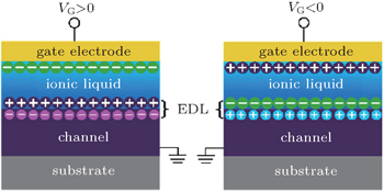
Field-effect transistors are indispensable for information processing and widely used in electrical control of magnetism. In the FET, the capacitance (C) of the insulating layer determines the change in carrier density ΔnS (ΔnS ∼ CVG/e; VG is gate voltage and e is the electron charge). To realize a larger ΔnS without increasing VG, the enhancement of C = κε0/d (κ is the relative permittivity, ε0 is the vacuum permittivity, and d is the thickness of the dielectric layer) is an effective route.[113] A conventional approach to obtaining a large C is to adopt high κ materials (e.g. Al2O3, HfO2, or ZrO2) with a thickness of ∼ 50 nm by atomic layer deposition. Alternatively, ionic liquid consisting of anions and cations could produce an electric double layer (EDL) (pairs of sheets of negative and positive charges) at the interface between ionic liquid and the channel under electric field. The EDL has a very large C because size of the gap between the two charged sheets, which corresponds to d, is on the same order as the sizes of the anions and cations, as shown in Fig.
 | Fig. 7. Schematic diagram of the device structure of EDL under positive (left) and negative (right) gate voltage. |
EDL gating is used mainly in electrical manipulations of superconductivity, two-dimensional conductivity, and metal-insulator transition. Ueno et al. found electric-field-induced superconductivity in the insulating SrTiO3 by using EDL in KClO4-PEO.[114] The sheet carrier density was enhanced from zero to 1014 cm−2 and a two-dimensional superconducting state emerged below a critical temperature of 0.4 K under a gate voltage (VG) of 3.5 V. The EDL also brings about significant modulations of carrier density and sheet resistance in two-dimensional conductive systems such as LaAlO3/SrTiO3,[115] graphene,[116] and MoS2.[117] Nakano et al. found that a VG applied on vanadium dioxide (VO2) through DEME-TFSI can drive all the previously localized charge carriers in the bulk material into motion, leading to the emergence of a three-dimensional metallic ground state.[118] A voltage-sweep measurement showed that the metal–insulator transition provides a non-volatile memory effect, which is operable at room temperature. Also, metal-insulator transitions in other systems like SmCoO3,[119] NdNiO3,[120] Ca1−xCexMnO3,[121] etc., have been realized by electrical means using ionic liquid. More recently, the magnetism in both metal and oxide systems is electrically tuned by EDL gating. For instance, Weisheit et al. and Wang et al. manipulated the coercivity in FM FePt (FePd) and exchange spring in AFM IrMn, utilizing EDL gating, respectively.[7,122] However, the mechanism of EDL gating is under intense debate: is it electrostatic doping or electrochemical reaction? In the following, we will discuss the electrical control of magnetism in oxides with different mechanisms.
According to the conventional understanding from the capacitor model, the electric field only changes the carrier density (ΔnS ∼ CVG/e) in the system by an electrostatic doping mechanism. Dhoot et al. studied electrostatic field-induced doping in LCMO (x = 0.2) transistors using electrolyte (EMIM-TFSI) as a gate dielectric, as shown in Fig.
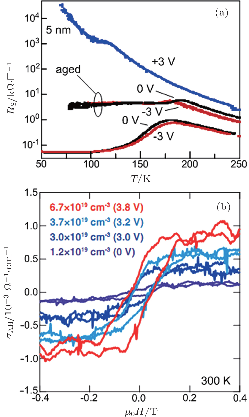 | Fig. 8. (a) Sheet resistance versus temperature for 5-nm LCMO (x = 0.2) at VG = 0 (black line), −3 (red line), and +3 V (blue line).[123] (b) Magnetic field dependence of the anomalous Hall conductivity σAH at 300 K for Co: TiO2, measured at different VG. The values of electron density n at each VG obtained from the ordinary Hall effect are shown in parentheses.[125] |
In another system, magnetic oxide semiconductor of Co:TiO2, Yamada et al. realized electric field–induced ferromagnetism at room temperature by means of EDL gating with high-density electron accumulation (> 1014 per square centimeter).[125] By applying a gate voltage of a few volts, a low-carrier paramagnetic state was transformed into a high-carrier ferromagnetic state, thereby revealing the considerable role of electron carriers in high-temperature ferromagnetism and demonstrating a route to room-temperature semiconductor spintronics, as shown in Fig.
Although the electrostatic doping mechanism successfully accounts for the changes in carrier density in some systems, it cannot explain the non-volatile electric-field effect in the whole bulk of film. Thus another mechanism base on electrochemical reaction is then proposed: the electric field applied on ionic liquid could bring about redox in the channel material, which could induce the creation and migration of oxygen vacancies.[127] The introduction of oxygen vacancies makes the non-volatile and in-depth effect reasonable.
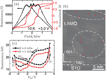
For example, the electrically reversible control of ferromagnetic phase transition based on oxygen vacancy migration in manganite film was reported by Cui et al.[20] The formation of an insulating, magnetically hard phase induced by the migration of oxygen in the magnetically soft matrix was directly observed in the magnetoresistance [Fig.
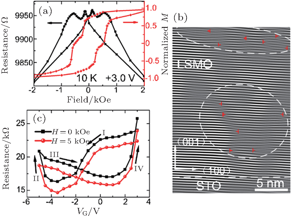 | Fig. 9. (a) Channel magnetoresistance acquired by sweeping the magnetic field along the channel (left axis) and the normalized magnetization curves measured with the magnetic field applied in-plane along the (100) direction of the substrate at 10 K under VG = + 3 V. (b) Fourier-filtered images of LSMO with VG = + 3.0 V. The ⊥ and dashed ovals mark the dislocation and estimated areas with high dislocation density, respectively. (c) Channel resistance versus VG with H = 0 kOe and 5 kOe.[20] |
Electrical manipulation of lattice, charge, and spin are realized respectively by the piezoelectric effect, field-effect transistor, and electric field control of ferromagnetism, bringing about dramatic promotions both in fundamental research and industrial production. However, it was generally accepted that the orbitals of materials were impossible to alter once they have been made. EDL gating was used to dynamically tune the orbital occupancy and corresponding magnetic anisotropy of LSMO thin films in a reversible and quantitative manner.[21] Positive gate voltage increases the proportion of occupancy of the orbital and the magnetic anisotropy that were initially favored by strain (irrespective of tensile versus compressive), while negative gate voltage reduces the concomitant preferential orbital occupancy and magnetic anisotropy (Fig.
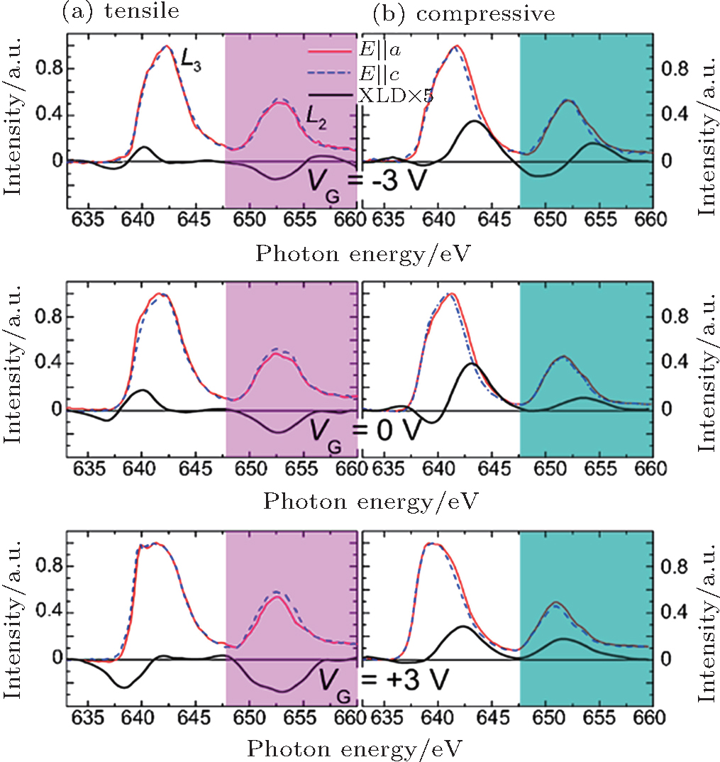 | Fig. 10. Normalized x-ray absorption spectroscopy (XAS) [photon polarization parallel (E ∥ a) and almost perpendicular (E ∥ c) to the sample plane] and x-ray linear dichroism (XLD) signals of (a) tensile and (b) compressive strained LSMO.[21] |
The electrochemical reaction mechanism was also demonstrated in the Co/GdOx, where the redox at the interface was controlled by the migration of oxygen ions under electric field.[129,130] The Co films could be reversibly changed from an optimally oxidized state with a strong perpendicular magnetic anisotropy to a metallic state with an in-plane magnetic anisotropy or to an oxidized state with nearly zero magnetization, depending on the polarity and time duration of the applied electric fields. Yuan et al. figured out a “phase diagram” to distinguish the electrostatic or electrochemical nature of EDL gating: the high work frequency and the low temperature together favor the electrostatic doping, while low frequency and high temperature favor the electrochemical reaction.[131] Nevertheless, various factors determine the mechanism of EDL gating, e.g. strain state, oxygen diffusion ability, etc., all of which need more in-depth investigation.
The two-dimensional electron gas (2DEG) or two-dimensional electron liquid (2DEL) that forms at the interface between the two insulating non-magnetic oxides LaAlO3 (LAO) and SrTiO3 (STO) has sparked widespread research interest due to its possession of a remarkable variety of emergent behaviors including superconductivity,[132,133] strong Rashba-like spin-orbit coupling[134] and ferromagnetism.[135–138] From a fundamental perspective, interfacial ferromagnetism could be a leading example of truly emergent phenomena; while it is true that bulk SrTiO3 can be doped to be metallic and superconducting, neither constituent in bulk form exhibits ferromagnetism.[138] The first signatures of magnetism at the LAO/STO interface were reported in magnetotransport measurements by Brinkman et al.[139] Direct current scanning quantum interference device (SQUID) magnetometry measurements by Ariando et al.[140] showed ferromagnetic hysteresis extending to room temperature. Torque magnetometry measurements by Li et al.[136] showed evidence for in-plane magnetism with a high moment density. Scanning SQUID microscopy by Bert et al.[137] revealed inhomogeneous micron-scale magnetic ‘patches’ x-ray circular dichroism measurements by Lee et al.[138] indicated that the ferromagnetism is intrinsic and linked to dxy orbitals in the Ti t2g band. Despite this variety of evidence, the existence and nature of magnetism in LAO/STO heterostructures has remained controversial. Since most of the exotic properties depend strongly on carrier density that can be tuned easily by electric field,[134] the nature of 2DEG or 2DEL can be readily explored by an electric field — back-gating[141] or top-gating[142] — or via nanoscale control using conductive atomic force microscope (AFM) lithography.[143]
At the LAO/STO interface, the electron gas is inherently sandwiched between two insulators. It is thus rather natural to try and explore the system’s ground states by modulating the carrier density with an electric field. In a standard field-effect device, an electric field is applied between a metallic gate and a conducting channel across a dielectric. SrTiO3 substrate is chosen as the dielectric because it is characterized at low temperatures by a large dielectric constant. The metallic gate is a gold film sputtered opposite to the channel area onto the back of the substrate. A typical sketch of the back-gated field-effect device is shown in the inset of Fig.
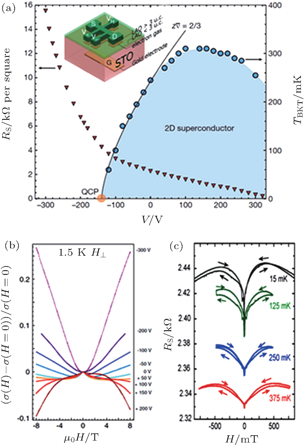 | Fig. 11. (a) Electronic phase diagram of the LAO/STO interface, obtained through field-effect modulation of the carrier density.[144] The inset shows a schematic view of a field-effect device, showing the source (S), drain (D), longitudinal voltage (V+ and V−), Hall voltage (VH), and gate voltage (G) contacts. (b) Modulation of the magnetoconductance s with gate voltage for an LAO/STO interface.[134] The change from a weakly localized regime (positive Δs) to a weakly anti-localized regime (negative Δs) reveals the increase in strength of the spin-orbit coupling. (c) Magnetoresistance (MR) at Vg ∼ 100 V at different temperatures.[145] |
Since the electronic properties of LAO/STO interfaces are extremely sensitive to growth conditions, some other samples prepared under higher oxygen pressure display coexistence of superconductivity and ferromagnetism.[145] Figure
Aside from back-gating, there is also top-gating of 2DEG by employing the dielectric of LAO film, which is often as thin as several unit cells and needs a much lower gating voltage. A two-terminal capacitor device is used to electrically gate the LAO/STO interface [Figs.
 | Fig. 12. (a) Experimental set-up: the MFM tip is mechanically driven by a piezoelectric transducer near its resonant frequency and kept at a constant height above the surface. The top electrode and the MFM tip are both grounded, and a DC bias is directly applied to the interface.[135] (b) Kelvin-probe force microscopy measurement of a region that includes the area for which MFM measurements are made.[134] The top gate is grounded, and voltage bias to the interface (Vdc) is 3 V. The topography is shown as height, while the colour maps onto the measured surface potential (the work function is already subtracted). (c) MFM frequency images over a 3 mm×3 mm area indicated by the black dashed line-enclosed region in panels (b). The MFM tip is magnetized horizontally parallel to the [010] sample direction.[135] MFM frequency images for Vdc increasing from −4 V to 0 V then decreasing to −4 V. Magnetic domain features are clearly observed for Vdc < − 2 V. The final state 2, obtained after cycling the voltage to Vdc = 0, is uncorrelated with the initial state 1. The regions enclosed by dashed lines give examples of where magnetic contrast is unchanged (region 1) or reversed (region 2) after voltage cycling. |
The discovery of electrically controlled ferromagnetism at the LAO/STO interface provides a new and surprising route to a wide range of spintronic applications. Nevertheless, the nature of the ferromagnetic state at the intriguing LAO/STO interface remains unexplored, and many effects such as spin-torque transfer, spin-polarized transport, and electrically controlled spinwave propagation and detection are expected but not demonstrated. Thus, there is plenty of space to employ the electric control in controlling interfacial ferromagnetism for the versatile application of the intriguing LAO/STO interface.
Controlling magnetization switching by an electric field without the assistance of a bias magnetic field may enable new data-storage spintronic devices requiring only low electric power. The modification of the correlated oxide interface may offer an avenue to explore this new strategy. In the experiments by Cuellar et al.,[146] the manipulation of interfacial magnetic Cu states with electric field in La0.7Ca0.3MnO3/PrBa2Cu3O7/La0.7Ca0.3MnO3 magnetic tunnel junctions [Fig.
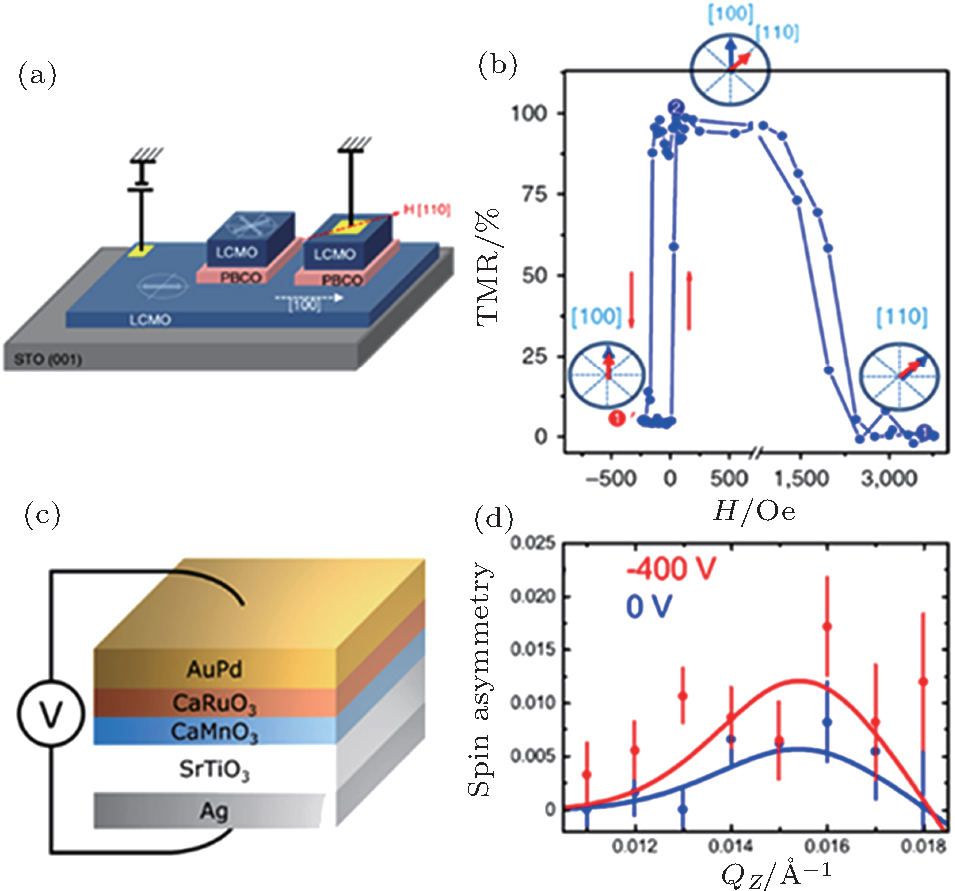 | Fig. 13. (a) Sketch of the LCMO (x = 0.3)/PrBa2Cu3O7/LCMO (x = 0.3) magnetic tunnel junctions and the test setup. Magnetic field was directed in-plane along the [110] direction (easy axis of the harder top layer), as according to drawing.[146] (b) At low bias (100 mV, blue symbols) the minor loop shows the saturation state 1, the high resistance state 2 (which is due to misalignment of magnetic moments of top and bottom layers), and the low resistance 1’ where magnetic moments are aligned along the easy axis of the bottom layer. Notice that high 2 and low 1’ resistance states are stable in zero magnetic field at a temperature of 94 K.[147] (c) Heterostructure and test setup schematics. (d) Spin asymmetry of Sample A after cooling in 700 mT without a bias and with a bias of −400 V, respectively.[147] |
Direct electric field control of magnetization without multiferroics or magnetoelasticity may also induce magnetoelectric coupling. Grutter et al. demonstrated an electric field dependence of the emergent ferromagnetic layer at CaRuO3/CaMnO3 interfaces [Fig.
Current information storage devices are based on two different aspects of solid state materials, spin and charge. Generally, spin and charge of electrons are employed separately. In magnetic recording and magnetoresistive random access memories (MRAM), a magnetic field (H) or a high-density current is used to write or read the information stored in the magnetization. Differently, the recording of two logic states (high resistive state HRS and low resistive state LRS) in resistive random access memories (RRAM) is on the basis of resistance switching modulated by electrical stimuli. The quest for higher data density in information storage is motivating researchers to study how to manipulate magnetization without the need of cumbersome H and achieve a new paradigm wherein spin and charge act on each other. Thus with a simple RRAM architecture, electrical control of magnetism in RRAM with the medium of diluted magnetic oxides,[148,149] antiferromagnet,[150,151] manganites[152,153] and ferrimagnets[154] has attracted extensive attention. The orderly migration of oxygen vacancies (VO) is considered to be the origin of the resistive switching (RS) behavior in these systems. Considering that such structures not only show stable bipolar RS characteristics, but also exhibit magnetic modulation with the alternation of set and reset processes, it is expected to obtain four logic states by encoding information in both RS and magnetic manipulation and even to achieve the dream of storing information magnetically and switching it electrically. Interestingly, magnetoresistance measurements indicate spin transport through an electrochemically formed copper nano-filament in LRS, in contrast to the disappearance of spin transport in HRS at the same temperature.[155]
In this review, we aim at illustrating the most recent progress in the electrical control of magnetism in oxides, but of course it is still very hard to cover all aspects, since this knowledge is continuing to develop so rapidly. The control of magnetism by ferroelectric switching in multiferroic heterostructures has focused mainly on strain, charge and exchange bias couplings to achieve an effective interaction between the magnetic and ferroelectric components of the composite system, giving rise both to magnetoelectric couplings much larger than those typical of intrinsic multiferroics and to functionalities that can in principle be optimized for device applications. The ionic liquid or EDL gating is a novel way to produce a dramatically large electric field using a voltage of only a few volts. The high permittivity and electric field in EDL gating enhance its ability in the manipulation of magnetism, reflected in the remarkable ferromagnetic-antiferromagnetic (paramagnetic) phase transition under electric field. The electric field applied on ordinary dielectric oxide could be used to control the exotic phenomenon originating from the charge transfer and orbital reconstruction at the interface between dissimilar correlated oxides. The electrical control of magnetism in oxides has become a popular topic of ever-increasing interest in the last decade; however, it is still in a quite infant stage, and thus many questions remain open with regard to both mechanisms and practical applications:
| 1 | |
| 2 | |
| 3 | |
| 4 | |
| 5 | |
| 6 | |
| 7 | |
| 8 | |
| 9 | |
| 10 | |
| 11 | |
| 12 | |
| 13 | |
| 14 | |
| 15 | |
| 16 | |
| 17 | |
| 18 | |
| 19 | |
| 20 | |
| 21 | |
| 22 | |
| 23 | |
| 24 | |
| 25 | |
| 26 | |
| 27 | |
| 28 | |
| 29 | |
| 30 | |
| 31 | |
| 32 | |
| 33 | |
| 34 | |
| 35 | |
| 36 | |
| 37 | |
| 38 | |
| 39 | |
| 40 | |
| 41 | |
| 42 | |
| 43 | |
| 44 | |
| 45 | |
| 46 | |
| 47 | |
| 48 | |
| 49 | |
| 50 | |
| 51 | |
| 52 | |
| 53 | |
| 54 | |
| 55 | |
| 56 | |
| 57 | |
| 58 | |
| 59 | |
| 60 | |
| 61 | |
| 62 | |
| 63 | |
| 64 | |
| 65 | |
| 66 | |
| 67 | |
| 68 | |
| 69 | |
| 70 | |
| 71 | |
| 72 | |
| 73 | |
| 74 | |
| 75 | |
| 76 | |
| 77 | |
| 78 | |
| 79 | |
| 80 | |
| 81 | |
| 82 | |
| 83 | |
| 84 | |
| 85 | |
| 86 | |
| 87 | |
| 88 | |
| 89 | |
| 90 | |
| 91 | |
| 92 | |
| 93 | |
| 94 | |
| 95 | |
| 96 | |
| 97 | |
| 98 | |
| 99 | |
| 100 | |
| 101 | |
| 102 | |
| 103 | |
| 104 | |
| 105 | |
| 106 | |
| 107 | |
| 108 | |
| 109 | |
| 110 | |
| 111 | |
| 112 | |
| 113 | |
| 114 | |
| 115 | |
| 116 | |
| 117 | |
| 118 | |
| 119 | |
| 120 | |
| 121 | |
| 122 | |
| 123 | |
| 124 | |
| 125 | |
| 126 | |
| 127 | |
| 128 | |
| 129 | |
| 130 | |
| 131 | |
| 132 | |
| 133 | |
| 134 | |
| 135 | |
| 136 | |
| 137 | |
| 138 | |
| 139 | |
| 140 | |
| 141 | |
| 142 | |
| 143 | |
| 144 | |
| 145 | |
| 146 | |
| 147 | |
| 148 | |
| 149 | |
| 150 | |
| 151 | |
| 152 | |
| 153 | |
| 154 | |
| 155 | |
| 156 |