† Corresponding author. E-mail:
Project supported by the National Key Basic Research Program of China (Grant No. 2011CBA00606), the Program for New Century Excellent Talents in University, China (Grant No. NCET-12-0915), and the National Natural Science Foundation of China (Grant Nos. 61334002 and 61404097).
Deep level transient spectroscopy (DLTS) as a method to investigate deep traps in AlGaN/GaN heterostructure or high electron mobility transistors (HEMTs) has been widely utilized. The DLTS measurements under different bias conditions are carried out in this paper. Two hole-like traps with active energies of Ev + 0.47 eV, and Ev + 0.10 eV are observed, which are related to surface states. The electron traps with active energies of Ec − 0.56 eV are located in the channel, those with Ec − 0.33 eV and Ec − 0.88 eV are located in the AlGaN layer. The presence of surface states has a strong influence on the detection of electron traps, especially when the electron traps are low in density. The DLTS signal peak height of the electron trap is reduced and even disappears due to the presence of plentiful surface state.
Trapping effect in AlGaN/GaN high electron mobility transistors (HEMTs) presents a major limitation to the power performance at high frequencies and the dynamic performance, for the density of two-dimensional electron gas (2DEG) is changed by the electrical charge trapped in the bulk and on the surface.
Deep level transient spectroscopy (DLTS), as one rapid, sensitive, and straightforward technology, has been utilized in GaN-based devices since 1994.[1] Three main native traps have been introduced: 0.15 eV–0.26 eV (E1),[2–4] 0.5 eV–0.61 eV (E2),[4–6] and 0.67 eV–0.89 eV (E3),[6,7] which are related to nitrogen vacancy, nitrogen antisite and nitrogen interstitial, respectively. The traps with responding to dopants have been investigated by some groups. C doping will introduce a new trap with an energy of Ec − 0.4 eV (CGa) and reduce the concentration of NGa.[8] Fe doping in the GaN buffer layer can induce a strong current collapse and increase the concentration of trap with an energy of Ec − 0.63 eV, which does not relate to the iron atoms but more likely to an intrinsic trap.[9] Sasikumar et al.[10] reported that the Ec − 0.45 eV trap was the dominant electrical stress-affected trap and likely caused the HEMT drain-lag and increased the mild knee-walkout. Deep levels induced by electron irradiation[11] and proton irradiation[12] have been investigated. Bisi et al.[13] summarized more than 60 papers and made a database of the deep levels in GaN- and AlGaN- based layers and devices. The DLTS measurement becomes more difficult as the structure of GaN- based devices is more complex. Look and Fang[14] investigated the method to distinguish the trap on the surface from that in the bulk for the GaN bulk material. However, it is not easy to directly detect the surface traps in the complex structure such as AlGaN/GaN heterostructure, while the charging and discharging of surface state has an important effect on the density of 2DEG in the channel and the DLTS measurement of traps in the channel. Okino et al.[15] reported the surface-state-related DLTS signals in AlGaN/GaN HEMTs by I-DLTS.
In this study, DLTS measurements are applied to AlGaN/GaN heterostructure with various reverse voltages, filling pulse voltages and widths. Hole-like traps are detected and related to surface states that affect DLTS signals of other electron traps.
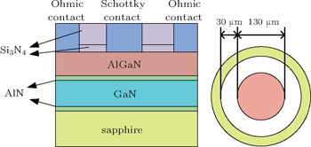
The AlGaN/GaN hetero-junction structure used in this paper was grown by metal-organic chemical vapour deposition (MOCVD) on a (0001) sapphire substrate. The epitaxial structure was composed of, from the substrate up, a nuclear layer, a 1.3-μm-thick unintentionally doped (UID) GaN layer, a 1-nm-thick AlN interlayer, and a 20-nm-thick unintentionally doped Al0.3Ga0.7N barrier layer. Circular shaped Schottky diodes were utilized for CV, IV, and DLTS measurements, each with a circular gate contact having a diameter of 130 μm and surrounding ohmic contact with an Ohmic–Schottky separation of 30 μm (as shown in Fig.
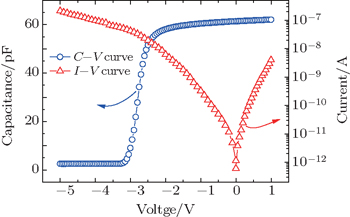
The C–V and I–V characteristics were measured at room temperature in the dark to characterize the devices and determine the voltage range applied in the DLTS measurements using the Semetrol DLTS system. The frequency of C–V and DLTS measurement was 1 MHz. The temperature range was from 45 K to 450 K in DLTS measurement.
The I–V and C–V characteristics are shown in Fig.
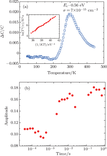
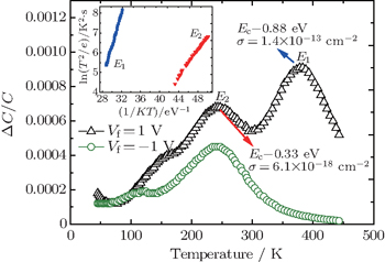
The DLTS spectrum measured in the pinch-off region (Vr = − 3 V, Vf = − 2 V, pulse width = 0.1 ms) is shown in Fig.
The pulse width dependence of the transient capacitance amplitude at 300 K is exhibited in Fig.
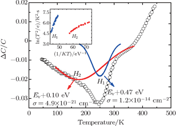 | Fig. 4. DLTS spectra with a rate window e = 133 s−1 and Arrhenius plots (inset) with Vr = − 3 V, Vf = − 2 V, and pulse width = 50 ms. |
The DLTS scan with 50-ms filling pulse and the same voltage settings as those in Fig.
Negatively going DLTS signals have been studied for GaAs metal-semiconductor field effect transistors and AlGaAs/GaAs HEMTs since 1986.[17–19] The hole-like trap signal can be explained by the variation in the population of surface states occupied by electrons. The Si3N4 layer directly passivates the deep donor state on the AlGaN surface, introduces large-density fast state traps,[20] and may be related to the incorporation of silicon atoms at the SiN/AlGaN interface,[21,22] which can explain the presence of H1 in Fig.
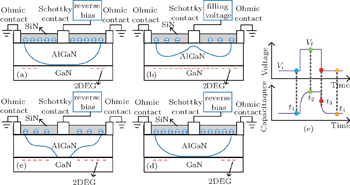
Ibbetson et al.[23] and Smorchkova et al.[24] proposed that surface donor-like traps are the source of the electrons in the channel, and the electrons are driven into the channel by the strong polarization field. Surface states can capture electrons to form a “virtual gate” on the ungated surface.[25] The response of the depletion region under the “virtual gate” is much slower than that under the real gate contact.
The transient behavior of the depletion region under the gate and surface is illustrated schematically in Fig.
When the gate switches to a filling pulse, gate depletion shrinks instantaneously, while the depletion region under an ungated surface cannot respond to gate voltage immediately, for it takes a longer time to emit electrons from the surface states as the process between t1 and t2 in Fig.
When the filling pulse switches to reverse bias, the virtual gate effect becomes stronger again and the surface states restart to capture electrons. The relatively slow capture process gives rise to the decreasing of capacitance due to the reduced 2DEG between t3 and t4 as shown in Figs.
Figure
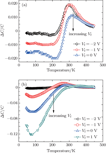 | Fig. 6. DLTS spectra measured each as a function of filling pulse height with a rate window e = 133 s−1 when pulse width is 0.1 ms. (a) Vr is −3 V and (b) Vr is −2.7 V. |
It seems that the concentration of hole-like traps in Fig.
Our measurements show that the negative signal does not appear when reverse voltage is −2 V and pulse width is 0.1 ms. E1 (Ec − 0.88 eV, σ = 1.4 × 10⁻¹³ cm−2) and E2 (Ec − 0.33 eV, σ = 6.1 × 10⁻¹⁸ cm−2) are detected and shown in Fig.
The DLTS measurements under different bias conditions are carried out in this paper. Hole–like traps are detected as a result of surface states emitting and re-capturing electrons. The DLTS signal peak height of the electron trap is reduced and even disappears with the advent of plentiful surface states. Suppression of surface states is very important for not only optimizing the performance of the device but also improving the veracity of electron trap DLTS measurements in AlGaN/GaN heterostructure. In addition, traps on the surface need to be further investigated in order to be controlled better.
| 1 | |
| 2 | |
| 3 | |
| 4 | |
| 5 | |
| 6 | |
| 7 | |
| 8 | |
| 9 | |
| 10 | |
| 11 | |
| 12 | |
| 13 | |
| 14 | |
| 15 | |
| 16 | |
| 17 | |
| 18 | |
| 19 | |
| 20 | |
| 21 | |
| 22 | |
| 23 | |
| 24 | |
| 25 | |
| 26 | |
| 27 | |
| 28 |


