†These authors contributed equally to this work.
‡Corresponding author. E-mail: jinglu@pku.edu.cn
*Project supported by the National Natural Science Foundation of China (Grant Nos. 11274016, 11474012, and 1207141) and the National Basic Research Program of China (Grant Nos. 2013CB932604 and 2012CB619304).
Free standing silicene is a two-dimensional silicon monolayer with a buckled honeycomb lattice and a Dirac band structure. Ever since its first successful synthesis in the laboratory, silicene has been considered as an option for post-silicon electronics, as an alternative to graphene and other two-dimensional materials. Despite its theoretical high carrier mobility, the zero band gap characteristic makes pure silicene impossible to use directly as a field effect transistor (FET) operating at room temperature. Here, we first review the theoretical approaches to open a band gap in silicene without diminishing its excellent electronic properties and the corresponding simulations of silicene transistors based on an opened band gap. An all-metallic silicene FET without an opened band gap is also introduced. The two chief obstacles for realization of a silicene transistor are silicene’s strong interaction with a metal template and its instability in air. In the final part, we briefly describe a recent experimental advance in fabrication of a proof-of-concept silicene device with Dirac ambipolar charge transport resembling a graphene FET, fabricated via a growth-transfer technique.
One of the most attractive characteristics of graphene is its ultra-high electron mobility of 2 × 105 cm2/V· s, [1, 2] while the mobility of the bulk silicon currently used in industry is only 103 cm2/V· s at room temperature. This makes graphene a very promising candidate material for fast transistors and high-frequency operation. However, pure graphene is not suitable for effective field-effect transistors (FET) operating at room temperature, due to its zero band gap. Opening a sizable band gap without diminishing graphene’ s other useful electronic properties is critical for the application of graphene in nanoelectronics, and it is one of the most important and tantalizing research topics of the graphene community. Any successor to silicon metal-oxide-semiconductor FETs (MOSFET) that are used in complementary MOS-like logic must have a sizeable band gap of 0.4 eV or more and an on– off current ratio between 104 and 107.[3] Unfortunately, the band gap opened in graphene without degrading other electronic properties (via a vertical electric field, molecular surface adsorption, or hexagonal boron nitride (h-BN) substrate)[4– 7] is usually smaller than 0.34 eV, and the observed on– off current ratio at room temperature is no greater than 100.[8]
Silicene is predicted to be a zero band gap semiconductor with a Dirac cone like that observed in graphene. Due to silicene’ s massless Dirac fermions, high carrier mobility is calculated to be on the order of 103 cm2/V· s (electron– phonon interaction included).[9] Therefore, silicene is a promising material for high-speed switching devices. It is readily apparent that pure silicene cannot be used directly for effective FETs for the same reason that graphene cannot.
Although covalent functionalization or epitaxial growth in the form of nanoribbons can open a sizable band gap in silicene, other desirable electronic properties are simultaneously diminished — carrier mobility is inevitably decreased to a large extent, as happens in graphene. Therefore, opening a sizable and tunable band gap in silicene without degrading electronic properties is desired crucial hurdle for achieving high-performance silicene FET devices. So far, two mechanisms have been demonstrated to open a band gap in silicene while preserving its electronic properties: breaking of inversion symmetry and intervalley interaction. Applying a vertical electric field to the silicene layer is a typical way to open the band gap by breaking the symmetry between the two sublattices.[10] Creating a silicene nanomesh[11] by digging holes in silicene is a representative way of opening a band gap by intervalley interaction without diminishing valuable electronic properties. Surface adsorption[12] is also a typical way to open a band gap in silicene without diminishing electronic properties — both the aforementioned mechanisms are involved, as will be explained later in detail.
Due to the buckled structure of silicene, the application of a vertical electric field will cause a difference in the electrostatic potential of its two sublattices. Thus the inversion symmetry between the two sublattices is broken, and a direct band gap Eg is opened at the K point in the Brillouin zone.[10] The opened band gap increases linearly with E⊥ , as has been shown by density functional theory (DFT) calculations (see Fig. 1(d)). This linear dependence of Eg on E⊥ can be well explained in terms of a tight binding (TB) model calculation, which gives Eg = eE⊥ Δ (Δ is the buckling in a silicene layer).[10, 13] Band structures of silicene around Ef at three different amplitudes of vertical electric fields (E⊥ ) are displayed in Fig. 1. The band gap is Eg = 0.08 eV for silicene under E⊥ = 0.51 V/Å and is doubled under E⊥ = 1.03 V/Å . The effective mass of electrons in silicene monolayer at E⊥ = 0.4 V/Å (

 | Fig. 1. (a)– (c) Band structures of silicene around Ef at three different vertical electric fields. Inset in panel (a): band structures in the first Brillouin zone at E⊥ = 0. The Fermi level or the valence band top is set to zero. (d) Dependence of band gap and charge transfer on the electric field. Adapted with permission from Ref. [10]. Copyright 2012 American Chemical Society. |
Surface adsorption of alkali atoms is an effective way to open a band gap in silicene, based on mechanisms of both inversion-symmetry breaking and intervalley interaction. First, the adsorption of alkali metal (AM) atoms leads to a charge transfer between AM and silicene, which builds a perpendicular electric field in silicene. This perpendicular electric field breaks the sublattice symmetry and thus opens a band gap in silicene. The asymmetry between the two sublattices increases with the increasing coverage and the band gap is correspondingly increased. Here we would like to emphasize that the interaction between the alkali atoms and silicene is mainly of ionic character, which will not diminish the Dirac cone of silicene too much. Covalent interactions, such as the interaction between Ag substrate and a silicene layer, are so strong that they will destroy the Dirac cone and degrade the carrier mobility in the silicene.
Second, when the supercell takes the form of (√ 3 × √ 3)n or (3 × 3)n (n is an integer), intervalley scattering also plays a role to open the band gap. The AM atoms expand the lattice period and shrink the period in the corresponding Brillouin zone (BZ). As shown in Fig. 2(c), the reduced BZ of the Na-adsorbed silicene ((√ 3 × √ 3) silicene supercell) is colored green, and purple indicates the BZ of primitive silicene. Both the two inequivalent Dirac points of silicene Ks and 

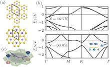 | Fig. 2. Sodium atoms adsorbed silicene layer: (a) Optimized geometry, (b) band structures. The Na atom coverage is 16.7% and 50.0% respectively. The Fermi level is set to zero. Inset in the bottom of panel (b) is orbital of the conduction band bottom at the Γ point. (c) The k-space of the AMSi6 supercell (one Na atom on (√ 3 × √ 3) silicene). The Brillouin zones of pure silicene and AMSi6 monolayer are colored purple and green, respectively. Adapted with permission from Ref. [12]. Copyright 2012 Nature Publishing Group. |
Besides alkali atoms, adsorption of transition atoms can also open a sizeable band gap at the Dirac point of silicene without degrading its electronic properties.[14] The size of the gap ranges between 0.03 eV and 0.66 eV, depending on type and coverage of dopants. More intriguingly, while alkali metal atom adsorption can induce only n-type doping in silicene, transition metals can induce different types of doping (n-type by Cu, Ag, and Au adsorptions, p-type by Ir adsorption, and neutral type by Pt adsorption).
The third novel method to open the band gap of silicene is to make a periodic array of holes in the silicene, i.e., fabricate silicene nanomesh (SNM). The SNM model is built by digging a simple triangular array of hexagonal holes in a silicene sheet, as shown in Fig. 3(a). Each type of SNM is designated by the notation [R, W], where the R index reflects the radius of the hole, calculated by Nremoved = 6R2 (Nremoved is the number of Si atoms removed from one lattice cell), and the W index is the width of the wall between nearest-neighbor holes. Theoretical calculations show that an SNM behaves semimetallically like pristine silicene when W is odd (Fig. 3(b)). While if W is even, the band gap of silicene hexagonal nanomeshes is opened at the Γ point, as shown in Fig. 3(c). The opened band gap when W is even monotonically decreases with increasing W, given the same R. A maximum band gap of about 0.68 eV is observed in both the R = 1 and 2 cases (Fig. 3(d)). SNM’ s mechanism of band gap opening is similar to that of GNM. It originates in geometric symmetry.[15, 16] In [R, W] SNM, when W is even, its two reciprocal lattice vectors overlap with Dirac points of pristine silicene, i.e. the K and K′ points of pristine silicene are folded into the Γ points of SNM.[4, 6, 15, 16] Degeneracy at the Dirac points is lifted and a sizable band gap appears. Otherwise, it is semimetallic-like silicene.
Similar to graphene nanomesh (GNM), [17] the band gap Eg in SNM when W is even is determined by the relation

where Ntotal and Nremoved are, respectively, the number of Si
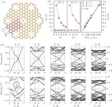 | Fig. 3. (a) Geometric configuration of SNMs with R = 1 and W = 4. Yellow and white balls represent Si and H atoms, respectively. Energy band structures of SNMs with odd (b) and even (c) W. (d) The band gap of SNM as a function of W with R = 1 and 2. (e) Band gap is plotted versus the quantity  |

The application of silicene in an FET was theoretically investigated by Lu’ s group.[10] A dual-gated silicene FET with SiO2 dielectric and h-BN buffer layer was constructed (Fig. 4(a)). The dual gate in this device allows control of both the doping level and the vertical electric field applied to the monolayer. The vertical electric field applied to the silicene can be written as E⊥ = (Vt − Vb)/(d0 − 2di+ 2di/ɛ ). The corresponding total gate voltage is Vg = Vt+ Vb, reflecting the total doping level. Under zero vertical electric field, there is a transmission “ bulge” around Ef inside the bias window at Vg = − 0.2 V (Fig. 4(b)). However, under external field of E⊥ = 1 V/Å , an obvious transport gap of about 0.14 eV is opened. Under Vg = 1 V, the transport gap moves away from the bias window, resulting in the recovery of the bulge, and the device is turned from off-state to on-state. The on/off current ratio under E⊥ = 1 V/Å is 4.2 at 300 K. The low on/off current ratio may be caused by the short channel (∼ 67 Å ), which gives rise to a larger leakage current in the off-state due to tunneling.
In light of the reactive nature of sp3-hybridized silicene, the dielectric should be carefully chosen. Silicene spontaneously forms covalent bonds with both Si and O atoms on the common SiO2 dielectric. However, both silicene and h-BN are approximately intact when placed on or sandwiched between h-BN even under an electric field of up to 2 V/Å . Therefore, insertion of an h-BN buffer layer between silicene and an oxide substrate is strongly recommended in a silicene FET device to maintain the structural integrity and high carrier mobility.
Besides the use of the h-BN layer, other substrates — such as hydrogenated Si-terminated SiC (0001) surface, graphane, and MoS2 — also interact with silicene via weak van der Waals (vdW) forces.[18– 21] Thus silicene can retain its
 | Fig. 4. Dual-gated silicene FET: (a) schematic model, (b) transmission spectra, and (c) projected density of states of the channel under different gate voltages and electric fields with a fixed Vbias = 0.1 V, obtained from the GGA/SZ level. The dashed vertical line indicates the bias window. The channel length is ∼ 67 Å . The Fermi level is set to zero. (d) Transmission eigenstates for the off- and on-state (Vg = 0.2 V and 1 V, respectively) at Ef and at the (0, 1/3) point of k-space under E⊥ = 1 V/Å . The isovalues are 0.8 a.u. Reproduced with permission from Ref. [10]. Copyright 2012 American Chemical Society. |
geometric structure and excellent electronic properties according to ab initio calculations.[25, 26] The insertion of alkali atoms between silicene and a substrate can also preserve the Dirac cone of silicene, but this leads to strong n-type doping of silicene.[22]
The Dirac cone of silicene can also be preserved when the silicene is embedded between two graphene layers.[23] However, the hybrid system becomes metallic since both silicene and graphene are semimetallic with zero band gap and the minima of the projected density of states of the silicene and graphene layers do not coincide with each other. The superlattice of silicene and MoS2 monolayers, with alternate stacking of the silicene and MoS2 monolayers, exhibits a metallic character that differs from that of silicene on MoS2 substrate.[24]
As discussed above, a sizable band gap up to 0.5 eV can be opened in silicene sheet upon alkali metal adsorption. The on/off current ratio of an FET based on this alkali atoms-adsorbed silicene structure is thus expected to be much higher than that of a dual-gated silicene FET.[12] As shown in Fig. 5, the central region of the simulated FET is an NaSi2 monolayer with a length of 113.8 Å . The electrodes are composed of semi-infinite silicene. The dielectric region, with a thickness of 7 Å , consists of an SiO2 substrate and h-BN buffer layers to preserve the high carrier mobility of silicene. A bottom gate is placed below the dielectric region.
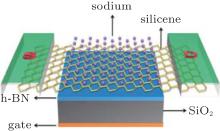 | Fig. 5. Schematic model of an FET based on the Na-covered silicene. The channel is 113.8 Å long, and the electrodes are composed of semi-infinite silicene. Reproduced with permission from Ref. [12]. Copyright 2012 Nature Publishing Group. |
When Vg = 0 V, the transport gap is located below Ef, and there is a broad transmission peak within the bias window (Fig. 6(a)). Hence, the FET is in the on-state with a current of 236 μ A/μ m. As depicted in the insets at the right of Fig. 6(a), Ef shifts downward with decreasing Vg. When Vg = − 18 V, Ef moves closer to the transport gap. Accordingly, the peak in the transmission window becomes narrower and the current reduces to 18.0 μ A/μ m. When Vg = − 30 V, Ef is located in the gap region, and the transmission probability nearly vanishes within the transmission window. Consequently, an effective off-state with a tiny current of 5.45 × 10− 7 μ A/μ m is achieved. The switching effect is also reflected in the transmission eigenstate at Ef and k point = (0, 1/3), as shown in Fig. 6(b). The transmission eigenvalue in the on-state is 0.70, and the corresponding incoming wave function reaches the other lead with slight scattering. In contrast, the transmission eigenvalue in the off-state is merely 0.01, and the incoming wave function is unable to reach the other lead due to strong scattering. Figure 6(c) shows the transport characteristics of the NaSi2 monolayer FET, and they are typical of n-type doping. As expected, the on/off current ratio in this FET is very high (4 × 10⁸), meeting the requirement for high-speed logic applications.
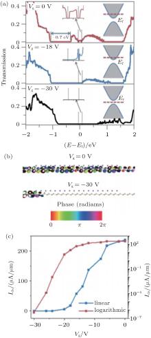 | Fig. 6. Device performance of an Na-covered silicene FET. The bias voltage is set to 0.1 V. (a) Transmission spectra with Vg = 0, -18, and -30 V, respectively. The vertical dashed line indicates the bias window. The details in the bias window are provided in the left insets. The right insets are sketches illustrating the relative positions of Ef and the gap manipulated by Vg. (b) Transmission eigenstates (at E = Ef and k point = (0, 1/3)) of the on-state (Vg = 0 V) and off-state (Vg = − 30 V). The isovalue is 0.2 a.u. (c) Transfer characteristic in linear (left axis) and logarithmic scales (right axis). Reproduced with permission from Ref. [12]. Copyright 2012 Nature Publishing Group. |
Metal atom adsorption can induce a larger band gap, up to 0.5 eV, in silicene, [12, 14] but a large supply voltage (Vdd) of about 30 V is required. It is highly desirable to design a new silicene FET with a high on/off ratio at low supply voltage. As discussed before, SNM has a maximum band gap of 6.8 eV, which is quite suitable for FET applications. Computing technology will require an FET channel length of less than 10 nm in the coming decades. It is a pretty intriguing possibility that the performance of sub-10-nm SNM FETs might satisfy the requirements of the International Technology Roadmap for Semiconductors (ITRS) for the next ten years.
A schematic model of a single-gated FET based on SNM is presented in Fig. 7(a). The electrodes are composed of semi-infinite silicene. The transfer characteristics of the sub-10-nm SNM FETs are provided in Fig. 7(b). Clear on/off current modulation is achieved. For the 9.1-nm SNM FET, if we set Vdd = Von − Voff = 0.5 V and Vg = 0.5 V is chosen as the on-state, the on/off ratio can reach 5.1 × 10⁴. This is about three orders of magnitude larger than the maximum on/off ratios obtained in dual-gated silicene FET, and it meets the requirement of 104∼ 107 for the high-speed logic applications. The subthreshold swing (here, SS is defined as dVgate/d(logI)) is 68 mV/dec, which approaches the 60 mV/dec switching limit of classical transistors. The on/off current ratio Ion/Ioff monotonously decreases from 5.1 × 10⁴ at Lgate = 9.1 nm to 17 at Lgate = 3.8 nm, showing a great short-channel effect. (The gate voltage window is limited to a supply voltage of 0.5 V.)
To support comparison of SNM FETs with Si-based and CNT transistors at a supply voltage Vdd = 0.5 V, the critical performance parameters of the sub-10-nm SNM (9.1 nm and 7.8 nm), advanced Si, and CNT FETs at Vbias = 0.5 V are offered in Table 1. The 9.1-nm SNM FET is competitive with the sub-10-nm advanced Si devices, but is inferior to the 9-nm CNT device. Adding to the total area of the gates is an effective way to strengthen the gates’ control over the channel. As shown in Table 1, the gate control ability of an FET is substantially improved by a dual gate configuration. The 9.1-nm dual-gated SNM performs better than the sub-10-nm advanced Si devices and the 9-nm CNT device. And the 7.8-nm dual-gated SNM performs better than the sub-10-nm advanced Si devices and is competitive with the 9-nm CNT device. The 9.1-nm and 7.8-nm dual-gated SNM FETs both deliver a high on-state current. Unfortunately, the on/off current ratios in the 9.1-nm and 7.8-nm dual-gated SNM FETs are only 1.8 × 10³ and 1.2 × 10³, respectively, neither of them meeting the requirements for HP logic in the ITRS (1.33 × 10⁴ in 2022 and 1.35 × 10⁴ in 2023).
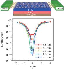 | Fig. 7. (a) Schematic diagram of an SNM FET structure. The yellow and white balls represent Si and H atoms, respectively. (b) Transfer characteristics of the SNM FETs for different channel lengths at Vbias = 0.2 V. Reproduced with permission from Ref. [11]. Copyright 2014 Nature Publishing Group. |
To include the phonon effect (only elastic scattering is considered), a molecular dynamics (MD) simulation of the channel region in a 9.1-nm single-gated SNM FET is performed at room temperature. When Vbias = 0.5 V, the on-state current is decreased to 4.0 μ A/μ m, and the on/off current ratio is decreased to 100. Therefore, SNM FETs still work at room temperature, but performance is greatly degraded. In summary, the sub-10-nm SNM FETs have excellent performance at zero temperature, but performance greatly degraded when the phonon scattering effect is included.
| Table 1. Comparison of performance metrics between sub-10-nm SNM, advance Si, and CNT transistors. |
Even though the alkali metal-adsorbed silicene FETs exhibit ultrahigh on/off current ratio, the required supply voltage Vdd is large. In fact, power dissipation has been a fundamental issue for nanoelectronic circuits. Compared with MOSFETs, tunneling FETs (TFETs) can have a smaller subthreshold swing and supply voltage Vdd, allowing for less power dissipation.
A silicene p– i– n TFET, composed with three types of doping in different regions of the silicene (Fig. 8), was simulated by Lu’ s group.[14] The calculated on-state current, SS, and supply voltage are 1000 μ A/μ m, 77 mV/dec, and 1.7 V, respectively. This much increased on-state current and reduced supply voltage together suggest that the power dissipation within the silicene TFET is far below that of traditional FETs.
As explained above, the on/off current ratio of silicene is very poor due to the zero band gap. This greatly limits the application of pure Dirac materials in electronics at room temperature. While the opening of the band gap in silicene is still underway and remains challenging, all-metallic FETs are alternative candidates for the application of silicene in nanoelectronics. A recent study by Lu showed that without opening their band gaps, the vertically stacked Dirac materials like silicene/graphene can be used directly in high-performance devices.[31] This is because in Dirac material heterostructures, electron transport from graphene to silicene and vice versa near Ef is forbidden without assistance of a phonon, due to momentum mismatch, as shown in Fig. 9(a).
 | Fig. 8. Schematic model of silicene TFET. The yellow silicon atoms form a sheet of monolayer silicene. The source and drain are Ir (blue atoms)/Cu (red atoms) doped silicene and thus are p+ /n+ type semiconductors with band gaps of about 0.3 eV and 0.2 eV, respectively. The central region, or the channel, is doped with Pt (black atoms) and thus is a neutral type semiconductor with a gap of around 0.3 eV. The concentration of the dopants in all parts of the device is fixed at 5.6% (TMSi18, TM = Cu, Pt, and Ir). A 0.5-nm thick HfO2 dielectric region is placed over the channel. A thin h-BN buffer layer is included to protect the silicene from the oxide. Reproduced with permission from Ref. [14]. Copyright 2014 Royal Society of Chemistry. |
 | Fig. 9. Graphene/silicene heterostructure and vertical FET: (a) Band structure. Green and red represent graphene and silicene components, respectively. (b) (E, kx)-dependent transmission probability. Inset: Dirac cones of graphene (green) and silicene (red) in the miBZ. (c) Schematic plot of single-gated heterostructured vertical FET. (d) Transfer characteristics at vds = 0.2 V. Reproduced with permission from Ref. [31]. Copyright 2014 WILEY-VCH Verlag GmbH & Co. KGaA, Weinheim. |
Although this silicene/graphene heterostructure is all-metallic, a large transport gap of over 0.4 eV is observed in an ab initio quantum transport simulation of a single-gated two-probe model, accompanied by a high on/off current ratio of up to 106 (Fig. 9(d)). Such an intriguing property in silicene/graphene heterostructures is robust with regard to relative rotation of the two Dirac materials and can also be found in silicene/germanene and homogenous twisted bilayer graphene (BLG). Therefore, an all-metallic junction can be a semiconductor, and a new avenue is opened for Dirac-material vertical structures in high-performance devices without opening the materials’ band gaps.
Simulation of FETs based on semiconducting armchair-edged silicene nanoribbons (ASiNRs) (Fig. 10) shows tunability of properties by width and length of the nanoribbon channels.[32] The band gap of silicene nanoribbon depends
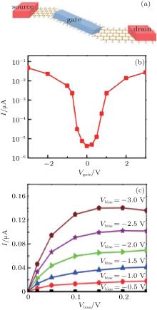 | Fig. 10. (a) A gated two-probe model constructed by an optimized 6-ASiNR connected to the 4-ZSiNR electrodes. The channel length is 4.62 nm. Yellow balls: Si; white balls: H. (b) Calculated transfer characteristics (Vbias = 0.02 V) of a 6-ASiNR (L = 9.89 nm) FET. (c) Calculated output characteristic of a 6-ASiNR (L = 9.89 nm) FET. The gate voltage varies from -0.5 V to -3.0 V in steps of 0.5 V. Reproduced with permission from Ref. [32]. Copyright 2012 Springer International Publishing AG. |
on the width of the nanoribbon, resembling the behavior of graphene. As a result, the on/off current ratio also shows a width dependence. In the same simulation, the on/off current ratio is observed to be positively related to the length of the channel in the checked range (44 Å ∼ 115.1 Å ). The SS, on the other hand, monotonously decreases with increasing L for a given ASiNR FET. In sum, high performance bipolar gate effects with an Ion/Ioff ratio of over 106 and an SS as small as 90 mV/decade are observed in intrinsic ASiNR-based FETs.
The calculated output characteristic of the ASiNR (L = 9.89 nm) FET is given in the bottom of Fig. 10. This is a typical FET output characteristic. That is, the currents first increase linearly (Vbias < 0.1 V) and then become constant (Vbias ≥ 0.1 V) with increasing bias voltage at the above-threshold region (Vgate ≥ Vth ≈ − 1 V). The saturated output characteristic is an advantage with respect to device speed. Whereas the output characteristics of many carbon-based (e.g., graphene, [33, 34] graphene nanoribbon, [35] and carbon nanotube[36]) FETs are linear with either no saturation or only weak saturation. The saturated output characteristic of the ASiNR-based FETs is a prominent disadvantage compared to carbon-based FETs. In SiNW-based FETs, either an output current saturated[37] or unsaturated characteristic can be obtained.[38, 39]
Despite recent theoretical progress of electronic devices based on silicene, it remains very challenging to realize these devices experimentally. This is because isolation of silicene from its template is difficult, and the exposed silicene is generally unstable in air, making it infeasible to transfer silicene via the widely used wet transfer technique. Tao and his coworkers specially pointed out the key role of Si– Ag interaction in stabilizing silicene.[40] First, they synthesized silicene by epitaxial growth on Ag (111) and added a 5-nanometer-thick layer of alumina on top. Then they peeled the silicene together with the Ag and alumina layers, and laid the sandwich on an SiO2 substrate with the Ag layer flipped up. In this way, the silicene layer can be preserved during transfer for device fabrication and measurements, avoiding the “ air stability issue” to some extent. Finally, they etched away part of the Ag to define the exposed silicene as the channel and the remaining native Ag film in the two ends as source/drain contacts. The whole synthesis– transfer– fabrication process is shown in Fig. 11(a).
As shown in Figs. 11(b) and 11(c), the silicene devices exhibited a Dirac-like ambipolar charge transport character, in agreement with predictions. The current on/off ratio in the silicene transistor is estimated to be on the order of 10. A band gap of ∼ 210 meV is calculated based on its residual carrier concentration of 8 × 109 cm− 2; this is comparable
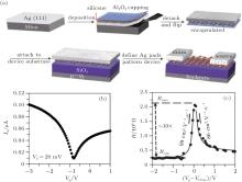 | Fig. 11. (a) Schematics of silicene and its synthesis– transfer fabrication process. (b) Drain current Id versus gate voltage Vg curve displays the ambipolar electron– hole symmetry expected from silicene. (c) R versus gate overdrive voltage (Vg– VDirac) of the silicene device. Measured transfer characteristics (dots) are in good agreement with a widely used ambipolar diffusive transport model (line). Reproduced with permission from Ref. [40]. Copyright 2015 Nature Publishing Group. |
with the band gap of graphene. The measured carrier mobility was ∼ 100 cm2 · V− 1· s− 1, one order less than the predicted intrinsic mobility of silicene. The substrate’ s effect on silicene is attributed to acoustic phonon-limited transport and grain boundary scattering.
In Table 2, we summarize the key performance parameters of silicene-based FETs. Theoretically, we are able to open a band gap in silicene without degrading its high carrier mobility and thus obtain high-performance silicene transistors. The experimentally achieved silicene FET shows an Ion/Ioff of 10 with a band gap of 0.21 eV. We believe that by taking full advantage of the proposed band gap opening methods, there is great potential for improving the performance of silicene FETs.
| Table 2. Performance of simulated and experimental silicene transistors. |
In the last decade, we have witnessed rapid development of 2D materials in the transistor community, including not only silicene and graphene but also MoS2 and black phosphorus. The great interest on the 2D materials stems mainly from their thinness, which makes them scalable to short gate lengths because of the optimal electrostatic control of the channel. For now, it is hard to say which material will win the race for future electronic applications. The two key advantages of silicene over other 2D materials are better compatibility with today’ s semiconductor industry and lower cost.
Theoretical studies suggest that it is possible to open a band gap in silicene without degrading its high carrier mobility and thus achieve high performance in silicene transistors. Experimentally, the main bottleneck is the difficulty of isolating silicene from its template and the instability of silicene when exposed to air, two vexing hindrances which make silicene very difficult to produce and work with. Even though these issues exist and silicene transistors remain far from mass production and commercial applications, it took only two and half years for the first silicene transistor to appear after successful synthesis of silicene on a metal template in 2012. Undoubtedly, this experimental breakthrough will strongly stimulate researchers in the field to continue looking for methods to solve the problems mentioned here. In the future, we expect mature techniques for extending the life of exposed silicene (exposed silicene degrades in about two minutes), large-scale manufacture of silicene, and intensified exploration of high-performance devices.
| 1 |
|
| 2 |
|
| 3 |
|
| 4 |
|
| 5 |
|
| 6 |
|
| 7 |
|
| 8 |
|
| 9 |
|
| 10 |
|
| 11 |
|
| 12 |
|
| 13 |
|
| 14 |
|
| 15 |
|
| 16 |
|
| 17 |
|
| 18 |
|
| 19 |
|
| 20 |
|
| 21 |
|
| 22 |
|
| 23 |
|
| 24 |
|
| 25 |
|
| 26 |
|
| 27 |
|
| 28 |
|
| 29 |
|
| 30 |
|
| 31 |
|
| 32 |
|
| 33 |
|
| 34 |
|
| 35 |
|
| 36 |
|
| 37 |
|
| 38 |
|
| 39 |
|
| 40 |
|


