†Corresponding author. E-mail: khwu@aphy.iphy.ac.cn
*Project supported by the National Basic Research Program of China (Grant Nos. 2012CB921703 and 2013CB921702), the National Natural Science Foundation of China (Grant No. 11334011), and the Strategic Priority Research Program of the Chinese Academy of Sciences (Grant No. XDB07020100).
Ag (111) is currently the most often used substrate for growing silicene films. Silicene forms a variety of different phases on the Ag (111) substrate. However, the structures of these phases are still not fully understood so far. In this brief review we summarize the growth condition and resulting silicene phases on Ag (111), and discuss the most plausible structural model and electronic property of individual phases. The existing debates on silicene on Ag (111) system are clarified as mush as possible.
Silicene is a single sheet of silicon atoms arranged in honeycomb lattice similar as graphene. It is a new two-dimensional (2D) silicon allotrope, different from any silicon structure previously found in nature. Silicene has attracted great interest, partially because of its similarity with graphene in both their structure and electronic properties. The study on silicene started with theoretical works. As early as 1994, Takeda and Shiraishi have proposed that silicon can exist in a two-dimensional sheet, [1] and also pointed out the key difference between silicene and graphene: In contrast to graphene where the A and B sublattices are in exactly the same plane, in silicene the two sublattices are relatively shifted in the direction perpendicular to the atomic plane, forming a so-called low buckled structure. However, this work was before the discovery of graphene and not paid too much attention. Following the boom of graphene research, silicene has received renewed interest. Several theoretical papers confirmed the buckled structure of silicene, [2, 3] and the name “ silicene” was also given.[2] Theoretical works also proposed various intriguing properties of silicene, including the existence of Dirac cone, [3, 4] and a larger spin– orbit coupling gap which can result in detectable quantum spin Hall effect (QSHE), [4] and unconventional properties tuned by external electric and magnetic fields[5, 6] as well as by nano-pattering, [7, 8] surface adsorption, [9, 10] and so on.
The breakthrough in experimental research on silicene took place in year 2012, when several groups reported in parallel the successful preparation of a silicene sheet. Among them Takamura group reported the formation of silicene on ZrB2 substrate, [11] whereas other groups, including the Le Lay group, [12] Kawai group, [13] and our group, [14, 15] reported the growth of silicene on Ag (111). It should be noted that before these works, Laimi et al. had claimed the successful growth of silicene on Ag (111) in an earlier work, [16] but their results were not reproduced by other groups. It was also notable that on Ag (111), silicene forms a variety of phases with different superstructures, including the 4× 4, 


Following the successful preparation of silicene, the focusing issue is then whether silicene indeed exhibits the exotic electronic properties predicted theoretically. To study the electronic structure of silicene, angle resolved photoelectron emission spectroscopy (ARPES) and scanning tunneling microscopy/spectroscopy (STM/STS) were two major experimental techniques. Le Lay et al. reported, together with their silicene structure, the ARPES measurement showing possible existence of the Dirac cone in the 4 × 4 phase of silicene.[12] However, their result was intensively questioned in the following few years.[21– 28] The key issue is that, once a monolayer silicene sheet is placed on a clean Ag (111) substrate, the interaction between the film and the substrate may significantly influence the surface electronic band structure. A number of theoretical papers argued that the Dirac state of silicene no longer exists.[21– 28] Additionally, the experimental work by scanning tunneling spectroscopy (STS) measurements by Lin et al. also found no signature related to a Dirac state.[21] The debates on this issue still continue, although at present most researchers tend to conclude that there is no Dirac state in this system. On the other hand, we mainly focused on the 
Another most concerned issue of silicene is whether a device based on silicene is possible. However, the study on silicene device meets great challenge, mainly because silicene is not as stable as graphene in air. Once exposed to air, it spontaneously oxidized and no longer exists. Also, currently all the substrates used for silicene are metallic, while for a device a semiconducting or insulating substrate is needed. The attempts to prepare silicene device started from a study on the protection layers, such as Al2O3.[32, 33] A breakthrough occurred recently, where Tao et al. reported an FET device based on silicene films grown on Ag (111), which shows ambipolar transport behavior.[34] This work should inspire more intensive study on silicene devices.
It is notable that, the silicene research is very challenging. The preparation of silicene usually required ultrahigh vacuum (UHV) environment, suitable substrates are difficult to find, and the surface is sensitive to oxidation. Certainly, making silicene devices is far more difficult than the case of graphene. Because of these difficulties, the study on silicene is still in its early stage, and severe debates exist in almost all aspects, including whether alloying occurs during growth, [35– 37] and whether Dirac state exists.[21– 28] These debates, however, should not stop the community from moving forward. Just think about the important fact: The silicon industry has been developed for decades and dominated our life, but a hexagonal silicon sheet, with graphene structure, has just been found in the last few years. One can imagine how strong impact it would have once the intriguing properties of silicene can be introduced to the existing silicon-based devices.
In this brief review, I do not intend to cover all aspects of silicene research. I will focus on a small but important topic, which is the entrance of the silicene world: the growth and atomic structures of silicene on Ag (111). Several years have passed since the silicene growth on Ag (111) was first reported, but there are still many controversies in literature concerning the different structures of silicene on Ag (111). On the other hand, due to the progress in silicene research, some previous unclear issues are now made clear, and so an update of misleading points in literature is necessary. In this mini-review, I will try to give a correct and comprehensive picture on the growth and structures of various silicene structures on Ag (111), covering all debating issues so that the readers would not be confused by conflicting literatures. I will mainly focus on experiment results and analyses. Theoretical calculations will be used mainly to help discussion and understanding.
The preparation of silicene film has to be conducted in UHV environment due to the sensitivity of Si upon oxidation. A clean Ag (111) substrate can be achieved by repeated argon ion sputtering and annealing process. Silicon is deposited by thermal evaporation from a pure Si source. The substrate temperature is the key that determines the structure of the resulting silicene film. Depending on the substrate temperature, a variety of reconstructed phases can be observed on Ag (111). When the substrate temperature is low, below about 400 K, silicon atoms deposited on Ag (111) tend to form clusters or disordered structures.[14] When the substrate temperature is above 400 K during deposition, the system experiences five ordered phases: T phase, 4× 4, 


So far, the report of different phases and discussion of their structural models in literature still remain controversy. For examples, the T phase is ascribed to a special 


The T phase, reported first by Feng et al., [14] was reproduced in a number of experimental papers, [38, 41] but it has been rarely discussed in literature. In STM images this phase appears as big and round protrusions arranged in a hexagonal closed pack pattern. The distance between neighboring protrusions is about 1.0 nm. Arafune et al. described it as 3.5× 3.5R26° reconstruction, but without detail analysis.[41] Liu et al. suggested that this phase has a periodicity and orientation identical to 

In our previous paper, [14] we ascribed this T phase as the “ precursor” for the formation of the 4 × 4 phase, the structure of this phase consisting of small pieces of silicene chips instead of a complete honeycomb lattice. Our model of the T phase is based on several experimental facts. Firstly, this phase does not appear in the same temperature regime with other ordered structures. It appears at the lowest temperature regime where ordered Si phases just appear on Ag (111). Although frequently one can observe coexistence of this phase with 4 × 4 and 


The first perfectly ordered phase observed at relatively low temperature is the 3 × 3 phase with respect to silicene 1 × 1, or 4 × 4 phase with respect to the Ag (111)-1 × 1 substrate. The 4 × 4 phase is very easy to recognize in STM images among all different silicene phases on Ag (111), thus it was first reported by several groups in parallel.[12– 14] The STM image of the 4 × 4 phase, as shown in Fig. 2, exhibits triangular half unit cells (HUC), each consisting of three bright spots, which is quite similar to the well-known Si (111)-5 × 5 surface structure. It is notable that between different 4 × 4 domains, one can often observe another phase with a 4 × 4 periodicity, namely the β -4 × 4 phase.[38] It should be noted that β -4 × 4 is not just a domain boundary structure, because the structure can extend to a few unit cell length, indicating a true periodic structure. The reason it appears in the domain boundaries between 4 × 4 phases may be that this phase is less stable than the normal 4 × 4 phase (hereafter noted as α -4 × 4), and that the strain in domain boundary can help to stabilize this phase. The STM images reveal that the two HUCs of the β -4 × 4 phase are different, one with six spots whereas the other has only one spot in the center (see Fig. 2(a)).
 | Fig. 2. The high resolution STM image and structural model of clean Si(3 × 3)/Ag(4 × 4)-α phase. (a) A typical STM image (14 nm× 11 nm in size). In the upper-right part of the image there is a small area consisting of a metastable-β phase. The white rhombus and the red rhombus mark the α -4 × 4 and β -4 × 4 unit cells, respectively. (b) Structural model of α -4 × 4. Each unit cell consists of 6 upper-buckled Si atoms and the two HUCs are mirror-symmetric (adapted from Ref. [15]). |
The atomic structure of the 4 × 4-α is relatively easy to be understood.[12] Although at the beginning some different models have been proposed, a general consensus has been reached. It has been known that there is a so-called “ magic mismatch” between the lattice constant of Ag (aAg = 2.88 Å ) and Si (aSi = 3.84 Å ), so that 4 × aAg = 3× aSi within 0.5% of error. Because both the Ag (111) surface and silicene are hexagonal lattices, the simplest model can be constructed by overlapping a low-buckled, free-standing silicene 1 × 1 lattice on top of an Ag (111)-1 × 1 lattice in the same orientation. This naturally results in a commensurate Si(3 × 3)/Ag(4 × 4) superstructure. The commensuration results in minimal interface strain and thus stabilizes the structure.
Overlapping two periodic lattices generally results in “ moiré pattern” , which is commonly observed in graphene on metal surfaces.[42– 45] But in the Si(3 × 3)/Ag(4 × 4) phase, the STM image showing six protrusions in each unit does not correspond to a moiré pattern. They are real Si atoms with higher position. This is due to the rearrangement of buckling configuration of Si atoms. Free-standing silicene-1 × 1 consists of two sub-lattices, A and B, just as the case of graphene. These two sublattices are displaced in opposite direction perpendicular to the film surface. However, once the silicene-1 × 1 sheet is placed on an Ag (111) substrate, the buckling configuration will spontaneously rearrange in order to lower the surface energy. In each Si(3 × 3)/Ag(4 × 4) unit cell there are 18 Si atoms, originally half of them are upper-buckled and half are lower-buckled. But after rearrangement only 6 Si atoms are upper-buckled, and other 12 Si atoms are all lower-buckled, see Fig. 2(b). Moreover, one can see that the 3 upper-buckled Si atoms in one HUC are not in the same sublattice with the 3 upper buckled Si atoms in the other HUC. This is in contrast to the case of free-standing silicene where all upper-buckled Si atoms (or all lower-buckled ones) belong to the same sublattice. Similarly, in the model of silicene β -4 × 4 phase, the registration of the silicene 1 × 1 lattice with the Ag (111) 1 × 1 lattice is identical to the α -4 × 4 phase. The only difference between them is the buckling configuration. In the β phase there are six upper-buckled Si atoms in one HUC, and only one upper-buckled Si atom in the other HUC. Totally there are 7 upper-buckled Si atoms in each UC (see Fig. 4(c)).
Recently, there have been questions on whether the experimentally observed silicene superstructures on Ag (111) is actually Ag– Si alloy phase. Prevot et al. explored in-situ STM measurement during the growth of silicene films, and found that the morphology of the Ag (111) suffers a significant change during growth.[35] They indicated that there is strong Ag mass transport during growth, and thus Ag atoms should be incorporated into the resulting silicene film. However, mass-transport is not a direct proof of the incorporation of Ag in the silicene film. So far, we believe that a pure silicene model without Ag incorporation is still the most plausible model. First, the atomic structure model of the silicene α -4 × 4 is a very natural one. It is energetically stable, and the simulated STM image can perfectly match the experimental observation. In fact, up to now there is still no alloy structure model that can explain the STM images of the 4 × 4 phase. In addition, recently we have conducted a hydrogen adsorption experiment, [46] which further supports the pure silicene structure model, as discussed below.
Hydrogen is the simplest atom. It tends to stick to un-saturated surface atoms with sp3 bonds, such as the Si (111) surface. The Si atoms in silicene have mixed sp2/sp3 hybridization, which weakens their π bond nature, so the Si atoms are partially un-saturated, and they will naturally adsorb one H atom to saturate its dangling bond. For free standing silicene, previous theoretical works proposed that hydrogenation of A and B sublattices from the two opposite sides of the silicene sheet is the most stable.[47– 49] However, on an Ag (111) substrate, only the top side of silicene is accessible to hydrogenation. In such a case the most favorable adsorption site would be the upper-buckled Si atoms. We hydrogenate the silicene α -4 × 4 phase by absorbing atomic hydrogen in UHV. Upon exposing to a saturate hydrogen dose at room temperature, a perfectly ordered structure with the same 4 × 4 periodicity can be observed, as shown in Fig. 3. High resolution image of the hydrogenated structure manifests two inequivalent HUCs, one with six bright spots while the other with only one bright spot in the middle, as shown in Fig. 3(b). The distance between the nearest bright spots is about 3.8 Å , corresponding to the lattice constant of silicene-1 × 1.
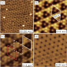 | Fig. 3. (a) A large area STM image of hydrogenated α -4 × 4 silicene surface showing an ordered 4 × 4 structure. (b) Zoom-in STM image of hydrogenated α -4 × 4 phase. The white rhombus marks an apparent unit cell of the structure. There are six bright protrusions in one HUC and one protrusion in the other HUC. (c) STM image showing the comparison between the position of apparent UCs of clean and hydrogenated α -4 × 4. The red and white rhombus correspond to clean α -4 × 4 UC and the hydrogenated α -4 × 4 UC, respectively. A translation of the white UC (dot line) does not match with the red one. (d) The clean α -4 × 4 surface is fully recovered after annealing the surface at 450 K (adapted from Ref. [46]). |
Since the adsorption of H atoms on upper-buckled Si atoms will only increase its degree of buckling, i.e., moves it a little bit upper. The resulting STM image with hydrogenation should be actually not much different from a clean silicene-α -4 × 4 surface. At a first glance this seems to contradict with our observation of significant change of the surface upon hydrogenation — the symmetric 4 × 4 HUCs become asymmetric. But interestingly, the STM image of hydrogenated α -4 × 4 phase looks very similar as the clean β -4 × 4 phase. Indeed, the buckling configuration of silicene changes from α -4 × 4 to β -4 × 4 after adsorbing H atoms. This is fairly easy to understand because in clean surface, the β -4 × 4 phase also prefers to stay in strained area — the domain boundaries between α domains. The adsorption of H atoms will increase the degree of buckling of Si atoms and thus increases the strain, and thus the β phase may become more stable. The perfect agreement of our theoretical model also supports that both the α -4 × 4 and β -4 × 4 are pure silicon structures, see Fig. 4. Indeed, after hydrogenation, one of the HUCs of the 4 × 4 structure becomes a local 1 × 1 structure, corresponding to 1 × 1 arrangements of Si atoms in a honeycomb lattice. There is simply no place to put possible Ag atoms in such a simple 1 × 1 lattice.
 | Fig. 4. Panels (a) and (b) are the structural model and the simulated STM image of hydrogen-terminated α -4 × 4 and β -4 × 4 models, respectively. Panels (c) and (d) are the structural model and the simulated STM image of hydrogen-terminated α -4 × 4 and β -4 × 4 models, respectively. In panel (c) the white and red rhombuses correspond to the positions of apparent UCs of α -4 × 4 and β -4 × 4 phases, respectively, which are shifted relatively. Note that in panels (a) and (c), the lateral position of Si atoms are fixed unchanged and only the buckling configuration has changed, resulting in the change of the position of apparent UCs (adapted from Ref. [46]). |
Another debating issue about the 4 × 4 phase is whether there exists Dirac electron states in the electronic structure. A number of theoretical and experimental evidences show that the Dirac state associated with a free-standing silicene no longer exists in a silicene film on Ag (111).[21– 28] However, interestingly, recently we have directly observed Dirac cones on a surface consisting silicene-4 × 4 on Ag (111) by ARPES.[50] The Dirac cones are present at the edges of the Brillouin zone, and there are twelve Dirac cones. This is in contrast to the theoretical expectation for free-standing silicene that involves six Dirac cones at the K (K′ ) points of the Brillouin zone. The unusual Dirac cone structure is an effect of the silicene– Ag (111) interface, and such interfacial effects may open up new possibilities for investigating quantum phenomena in low dimensional structures.

The 


The typical STM images of 


High resolution STM images reported by Liu et al. revealed the structure of the 


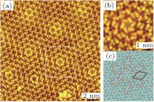 | Fig. 6. (a) High-resolution topography STM image taken on a  |
Similar as the 4 × 4 phase, the protrusions that one observed in STM images: the trimer and the spot at the corner, should correspond to rearrangement of the buckling of Si atoms. There have been a number of theoretical models proposed for this phase, [13, 21, 50– 53] as shown in Fig. 7. The simulated STM images were shown in the same figure. One can see that the models (a) and (e) both produce STM images quite similar as the experimental ones, and both of them are possible models. The difference between models (a) and (e) is simply an additional buckled Si atom (red ball). Taking into account the fact that upper-buckled Si atoms and lower-buckled Si atoms should naturally take alternative positions in a silicene lattice, model (a) is more reasonable, while in model (c) all the Si atoms in an HUC are lower-buckled, which should be energetically less favorable.

The 4 × 4 and 


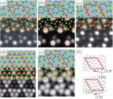 | Fig. 7. Summary of the atomic structural models proposed previously for the   |
A recent paper by Liu et al. claimed that this phase is too defective to be thermodynamically stable.[39] Here we emphasize that the phase is thermodynamically stable, but it is a challenging issue to understand its atomic structure, especially in the apparently disordered area. Note that recently, Tao et al. reported the FET devices based on monolayer silicene prepared on and then peeled off an Ag (111) substrate.[34] They selected 4 × 4 phase surface and (

Typical large area and zoom-in STM images of the Si(


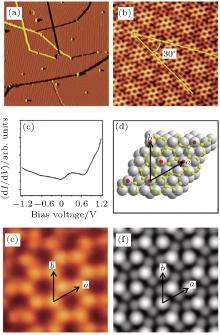 | Fig. 8. (a) A derivative STM image (200 nm× 200 nm, Vtip = 1.43 V) of a surface fully covered by the   |
The areas between ordered areas appear disordered and defective. However, carefully inspecting the disordered area, as shown in Fig. 9(a), one can find hidden order everywhere. Around a hole site there are always six spots, not more and not less. Connecting these six spots will result in a hexagon, albeit the hexagon is obvious distorted as compared with the perfect ones in the ordered center. Some of these six spots appear darker, which is the reason why the defective area appears darker than the perfect area. Therefore, although in our early paper we suggested that the large period pattern is due to moiré pattern, it should be more likely to be due to different electronic states in the ordered and disordered areas.
 | Fig. 9. (a) High resolution STM image of the (  |
We shall emphasize again that the disordered area is not completely disordered. It is most likely that the low-buckled honeycomb structure of silicene is distorted to accommodate the strain, but the basic honeycomb network is still preserved. Recently, Jamgotchian et al. proposed such a kind of structural model, [54] as shown in Fig. 9. Surrounding the perfect area are distorted hexagonal rings that corresponds to disordered area. The real situation should not be exactly same as this model, for example, we observe that the number of hexagonal rings in the perfect area is different from place to place. But the model indeed captures important ingredient of the system. In fact, we have recently conducted hydrogen adsorption experiment on the (


As the substrate temperature reaches 500 K, silicene islands with 


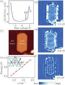 | Fig. 10. (a) dI/dV curves taken at 77 K. The position of Dirac point (DP) is labeled. (b) The STM image (40 nm× 40 nm) of 1-ML silicene surface containing an island of the second layer taken at tip bias − 1.0 V. (c), (d), and (e) dI/dV maps of the same area as panel (b) taken at tip bias − 1.0 V, − 0.8 V, and − 0.5 V, respectively. (f) Energy dispersion for silicene determined from wavelength of QPI patterns. The inset shows a schematic drawing of the overall band structure, with the relative location of DP, EF, and our data points (red line) (adapted from Ref. [15]). |
The STM image in Fig. 11 shows a silicene island across the step edges of the underlying Ag (111) surface without losing continuity, which is similar to graphene grown on metal surfaces. The high resolution STM image of Fig. 11(b) shows honeycomb structure of silicene terrace. The lattice period of the honeycomb structure is about 0.64 nm, corresponding to a 
To account for the atomic structure of the 
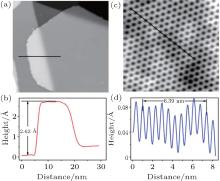 | Fig. 11. The STM image of a large area (65 nm× 65 nm) consisting of a sheet of silicene on Ag (111) crossing two substrate steps. (b) The line profile as indicated by the black line in panel (a) shows that the island is of one atom-thick. (c) The high-resolution STM image (10 nm× 10 nm) of the silicene surface taken at tip bias 1.0 V. The honeycomb structure is clearly observed. (d) The line profile as indicated by the black line in panel (c) showing both the lateral and vertical corrugations of the structure observed by STM (adapted from Ref. [15]). |
This structure of 


So far, there are several debating issues related with the 


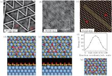 | Fig. 12. (a) and (b) The STM images of the same area on      |
The second debating issue is whether the 


In this brief review we summarized the growth condition and resulting silicene phases on Ag (111), and discussed the most plausible structural model and electronic property of individual phases. The existing debates on silicene on Ag (111) system are clarified as mush as possible. The key issue in the superstructure formation is the rearrangement of buckling which makes silicene potentially more controllable than graphene.
| 1 |
|
| 2 |
|
| 3 |
|
| 4 |
|
| 5 |
|
| 6 |
|
| 7 |
|
| 8 |
|
| 9 |
|
| 10 |
|
| 11 |
|
| 12 |
|
| 13 |
|
| 14 |
|
| 15 |
|
| 16 |
|
| 17 |
|
| 18 |
|
| 19 |
|
| 20 |
|
| 21 |
|
| 22 |
|
| 23 |
|
| 24 |
|
| 25 |
|
| 26 |
|
| 27 |
|
| 28 |
|
| 29 |
|
| 30 |
|
| 31 |
|
| 32 |
|
| 33 |
|
| 34 |
|
| 35 |
|
| 36 |
|
| 37 |
|
| 38 |
|
| 39 |
|
| 40 |
|
| 41 |
|
| 42 |
|
| 43 |
|
| 44 |
|
| 45 |
|
| 46 |
|
| 47 |
|
| 48 |
|
| 49 |
|
| 50 |
|
| 51 |
|
| 52 |
|
| 53 |
|
| 54 |
|
| 55 |
|
| 56 |
|
| 57 |
|
| 58 |
|
| 59 |
|
| 60 |
|


