A review of the growth and structures of silicene on Ag (111)
Wu Ke-Hui†a), b) 
A review of the growth and structures of silicene on Ag (111) |
|
Wu Ke-Hui†
|
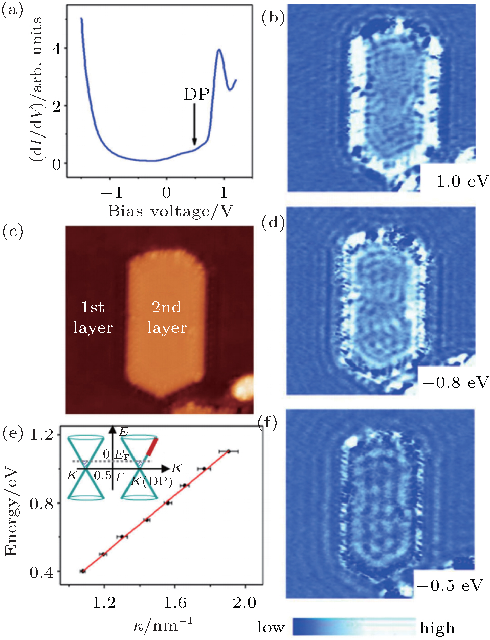
| (a) d I /d V curves taken at 77 K. The position of Dirac point (DP) is labeled. (b) The STM image (40 nm×40 nm) of 1-ML silicene surface containing an island of the second layer taken at tip bias −1.0 V. (c), (d), and (e) d I /d V maps of the same area as panel (b) taken at tip bias −1.0 V, −0.8 V, and −0.5 V, respectively. (f) Energy dispersion for silicene determined from wavelength of QPI patterns. The inset shows a schematic drawing of the overall band structure, with the relative location of DP, EF, and our data points (red line) (adapted from Ref. [ 15 ]). |
| |