†Corresponding author. E-mail: xcliu@mail.sic.ac.cn
*Project supported by the Innovation Program of the Chinese Academy of Sciences (Grant No. KJCX2-EW-W10), the Shanghai Rising-star Program, China (Grant No. 13QA1403800), the Industry–Academic Joint Technological Innovations Fund Project of Jiangsu Province, China (Grant No. BY2011119), and the National High-tech Research and Development Program of China (Grant Nos. 2013AA031603 and 2014AA032602).
A Ni/Ta bilayer is deposited on n-type 6H–SiC and then annealed at different temperatures to form an ohmic contact. The electrical properties are characterized by I– V curve measurement and the specific contact resistance is extracted by the transmission line method. The phase formation and microstructure of the Ni/Ta bilayer are studied after thermal annealing. The crystalline and microstructure properties are analyzed by using glance incident x-ray diffraction (GIXRD), Raman spectroscopy, and transmission electron microscopy. It is found that the transformation from the Schottky to the Ohmic occurs at 1050 °C and the GIXRD results show a distinct phase change from Ta2C to TaC at this temperature. A specific contact resistance of 6.5× 10⁻⁵ Ω·cm2 is obtained for sample Ni(80 nm)/Ta(20 nm)/6H–SiC after being annealed at 1050 °C. The formation of the TaC phase is regarded as the main reason for the excellent Ohmic properties of the Ni/Ta contacts to 6H–SiC. Raman and TEM data reveal that the graphite carbon is drastically consumed by the Ta element, which can improve the contact thermal stability. A schematic diagram is proposed to illustrate the microstructural changes of Ni/Ta/6H–SiC when annealed at different temperatures.
Silicon carbide (SiC) is a promising semiconductor material for high power, high temperature, high frequency electronic devices because of its unique material properties.[1– 3] SiC has been used to fabricate many kinds of power devices, such as high-voltage Schottky barrier diodes (SBDs), metal– semiconductor field-effect transistors (MESFETs), and photoconductive semiconductor switches (PCSSs).[4– 6] The electrical properties of metal/SiC have an important effect on the performance of a SiC power device. Industrial researchers have also explore the long-term use of SiC devices in radar, aircraft, and military communication systems in extreme environments.[7, 8] Moreover, a low contact resistivity and high thermal stablility Ohmic contact is very important for SiC devices.[9]
Ni based metallization has a relatively low work function and has attracted great attention in preparing Ohmic contacts to n-type SiC.[10– 12] High temperature annealing enables the chemical reaction between Ni and SiC to form nickel silicides. However, free carbon is also released at the interface of Ni/SiC.[13] Despite the outstanding electrical properties of Ni/SiC, the released carbon precipitate is an instable factor for the Ohmic contacts.[14] One solution to improve the contact stability is to use bilayer metallization to consume the released carbon precipitate.[15] Ta is a well-known refractory metal with a high melting point and remarkable mechanical properties. It can also react with C to form tantalum carbides. In addition, TaC has a higher melting point and lower resistivity than TiC, [16] which are the products of widely used Ni/Ti contacts to SiC that we have also reported, [17] this favors the high thermal stability and low Ohmic contact resistivity of the contacts. A very low specific contact resistance of 10− 6 Ω · cm2– 10− 7 Ω · cm2 has been obtained by Jang et al. by using TaC contacts to SiC.[18]
In this paper, we study the Ni/Ta bilayer contacts to ntype 6H– SiC. The thickness values of Ni and Ta layers are optimized and these layers are then annealed at different temperatures. The electrical properties, crystalline structure, and detailed chemical reaction process of Ni/Ta/6H– SiC are characterized and analyzed.
Commercial n-type 6H– SiC wafers with an electron concentration of 2.0 × 1018 cm− 3 were used. The transmission line model (TLM) method[19, 20] was used to characterize the electrical properties. Before depositing Ni/Ta bilayers, the SiC wafers were sequentially cleaned with deionized water, acetone, and a heated H2O2/NH4OH/H2O solution (mixture ratio: 1:1:5 and heated at 100 ° C). The SiC wafers were then dipped into 10 vol% HF acid for 15 s to remove the native oxide layer. TLM patterns were prepared on the Si-face of 6H– SiC substrate by the photolithography technique. Ta and Ni thin layers were subsequently deposited on 6H– SiC substrate by using the magnetron sputtering method. The contact pads were prepared by a lift-off process. The size of contact pad was 200 μ m× 100 μ m with different spaces of 5, 15, 25, 35, 45, 55, and 65 μ m. Finally, the Ni/Ta/6H– SiC were subjected to a rapid thermal annealing in Ar atmosphere for 2 min by using a rapid thermal processor (RTP 500). A series of Ni(80 nm)/Ta (20 nm) samples were annealed at 750 ° C, 850 ° C, 950 ° C, and 1050 ° C and labeled as NT-750, NT-850, NT-950, and NT-1050, respectively. A Keithley 4200 sourcemeter was used to measure the current– voltage (I– V) curve. The specific contact resistance was extracted by TLM. Glance incident x-ray diffraction (GIXRD) (Rigaku, D/max 2550 V) and Raman microscope (Renishaw, Invia Raman microscope) were used to analyze the phase formation. The interface microstructures were characterized by transmission electron microscope (TEM) (FEI, Tecnai G2 F20).
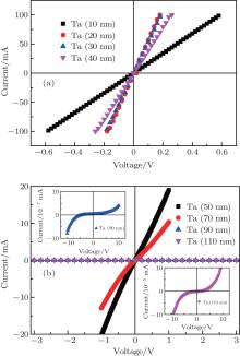
To optimize the thickness ratio between Ni and Ta, the effect of Ta layer thickness on the electrical properties of Ni/Ta/6H– SiC is investigated. Figures 1(a) and 1(b) show the measured I– V curves of Ni/Ta/6H– SiC with fixed Ni thickness of 80 nm and different Ta thicknesses, ranging from 10 nm to 110 nm. All of the samples were annealed at 1050 ° C for 2 min with a rapid thermal annealing process at Ar atmosphere. It can be observed that the I– V curves of samples with Ta thickness in a range from 10 nm to 40 nm are linear, while samples with Ta thickness ranging from 50 nm to 110 nm show parabola-like behaviors. The inset in Fig. 1(b) shows the zoomed parts of I– V curves of samples with the Ta thickness values of 90 nm and 110 nm in order to clearly present the parabola-like characteristic. The I– V curves indicate that Ni(80 nm)/Ta/6H– SiC exhibits Ohmic behavior when the Ta thickness is less than 40 nm, while it exhibits Schottky behavior as the Ta layer thickness increases.[21] The linear I– V curve for Ni(80 nm)/Ta(20 nm)/6H– SiC shows the maximum slope, which corresponds to a specific contact resistance of 6.5× 10− 5 Ω · cm2. Table 1 presents the specific contact resistance of Ni (80 nm)/Ta/6H– SiC annealed at 1050 ° C.
 | Fig. 1. I– V characteristic of (a) Ni(80 nm)/Ta (10, 20, 30, 40 nm)/6H– SiC (b) Ni(80 nm)/Ta (50, 70, 90, 110 nm)/6H– SiC annealed at 1050 ° C in Ar atmosphere for 2 min. |
| Table 1. Specific contact resistances of Ni(80 nm)/Ta/6H– SiC annealed at 1050 ° C for 2 min. |
The I– V curves of samples NT-750, NT-850, NT-950, and NT-1050 are shown in Fig. 2. In order to show more detail, the inset in Fig. 2 shows the I– V curves of sample NT-750 with zoomed Y axis. It can be clearly seen that the I– V curves of samples NT-750, NT-850, and NT-950 exhibit parabola-like characteristics, while sample NT-1050 shows good linear behavior. The I– V characterizations of Ni(80 nm)/Ta(20 nm)/6H– SiC mean that the annealing temperature plays an important role in determining the electrical properties. It shows a clear Ohmic contact property when annealed at 1050 ° C. The slope of I– V curve is gradually increased with increasing the annealing temperature from 750 ° C to 1050 ° C, which suggests a continuous reduction in contact resistivity or Schottky barrier height. Table 2 shows the contact types and specific contact resistances of Ni(80 nm)/Ta(20 nm)/6H– SiC when annealed at different temperatures.
 | Fig. 2. The I– V curves of samples NT-750, NT-850, NT-950, and NT-1050. The inset shows the zoomed part of I– V curve of sample NT-750. |
| Table 2. The contact types and the specific contact resistances of Ni(80 nm)/Ta(20 nm)/6H– SiC annealed at different temperatures. |
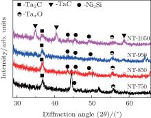
GIXRD is used to characterize the final compounds after annealing at different temperatures. Figure 3 shows the GIXRD patterns of samples NT-750, NT-850, NT-950, and NT-1050. It can be seen that Ni2Si, as the ubiquitous phase, exists in all samples since Ni2Si has the largest negative heat of formation.[22] It can also be identified that Ta2C and TaxO are present in all of the samples. The diffraction peak intensity of Ta2C gradually decreases as the annealing temperature increases from 750 ° C to 1050 ° C. A new diffraction peak corresponding to TaC appears when annealed at 1050 ° C. This implies that a higher annealing temperature (> 950 ° C) leads to a distinct phase transformation from Ta2C into TaC.
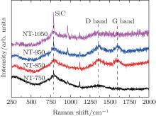
For the Ni-based contact to SiC, carbon precipitation is often produced during the chemical reaction and remains in the contact layer, which plays a crucial role in the electrical properties. In order to further investigate the remaining carbon phases in Ni/Ta/SiC structure, Raman spectroscopy is used to characterize the structural information. Figure 4 presents the Raman spectra of samples NT-750, NT-850, NT-950, and NT-1050. There are three main peaks in the Raman spectra, as marked in Fig. 4. The sharp peak located at 797 cm− 1 belongs to the 6H– SiC substrate. The other two broad bands centered at 1350 cm− 1 and 1580 cm− 1, chronically named D band and G band, correspond to the graphite carbon phase. The D band is related to disordered arrangement of six-fold aromatic carbon rings, while the G band originates from the E2g-symmetry phonon vibration in the Brillouin zone center of sp2-bonded carbon atoms.[23, 24] Only a broad D band is observed for sample NT-750. This indicates that the formed carbon is amorphous carbon when annealed at 750 ° C. After annealing at 850 ° C, a clear G band appears, which indicates that there is a graphitization process for the carbon phase. When the annealing temperature is increased to 950 ° C, the peak positions and intensities of D and G bands do not change very much. However, as the annealing temperature is further increased to 1050 ° C, the D and G bands completely disappear. This means that the amount of graphite carbon sharply decreases to an extremely low level, which is below the detection limit of Raman microscopy.
To have a direct insight into the microstructure evolution details in the annealing process, samples NT-750, NT-950, and NT-1050 are measured by using cross-sectional high resolution transmission electron microscopy (HRTEM). Figure 5(a) shows the low magnitude view TEM micrograph of sample NT-750. A smooth interface can be obviously observed, which indicates that there is a less violent chemical reaction between the Ni/Ta bilayer and SiC substrate. Figure 5(b) shows the selected area electron diffraction (SAED) patterns for the near interface position, marked as “ * ” in Fig. 5(a). Polycrystalline diffraction rings corresponding to Ni2Si and Ta2C phase are clearly observed to coexist with 6H– SiC single crystal diffraction lattice. This demonstrates that the Ta element still remains at the interface at this annealing stage. The cross-sectional morphologies of samples NT-950 and NT-1050 are shown in Figs. 5(c) and 5(e). It can be seen from Fig. 5(c) that the dominated phase of Ni2Si is also detected and the interface becomes very rough due to the severe chemical reaction. A more notable phenomenon shows that there is a well defined graphite carbon band with white contrast that exists at the interface. This agrees well with carbon signals shown in Raman spectra. The HRTEM micrograph in Fig. 5(d) subtly exhibits this typical fine structure at the interface. At this annealing temperature, Ta element is observed at the top of contact layer and in the forms of Ta2C and TaxO. As the annealing temperature increases to 1050 ° C, no white graphite band is found in or near the interface region. In addition, only a few dispersive graphite grains are identified near the surface region. According to the morphology feature and Raman results of sample NT-1050, it can be concluded that the amount of previously formed graphite carbon indeed decreases to an extremely low level. Meanwhile TaC, which is more thermodynamically favorable than Ta2C, is observed at the top of contact layer. Figure 5(f) presents the HRTEM micrograph of the position marked as “ + ” in Fig. 5(e). A lattice fringe that belongs to TaC grain is clearly observed on the top of Ni2Si phase.
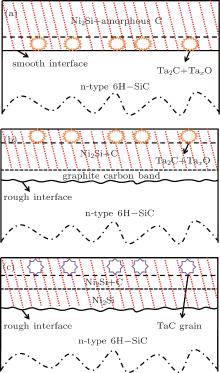
The microstructural evolutions of Ni/Ta bilayer contacts to 6H– SiC after annealing at different temperatures are schematically shown in Fig. 6. The chemical reaction can be separated into three stages. At the initial stage with an annealing temperature of 750 ° C, Ni diffuses through Ta layer to react with SiC substrate and then forms Ni2Si and Ta2C. The following chemical reaction takes place:

At this annealing temperature, Ta element still remains at the interface of Ta/SiC. Carbon is released from SiC substrate and exists in the form of amorphous carbon. In the second stage of annealing at 850 ° C and 950 ° C, the same phases are detected, while the released amorphous carbon is transformed into graphite carbon. In addition, the graphite grains are aggregated into a well defined graphite band directly coming into contact with the SiC substrate. Owing to further diffusion of Ni species, Ta related compounds out-diffuse to the top of contact layer. In the final stage with a high annealing temperature of 1050 ° C, Ta2C changes into TaC phase. This indicates that the following thermodynamic favorable reaction occurs:

A sharp consumption of graphite carbon happens at this stage, which is beneficial to the thermal stability of Ni/Ta Ohmic contact to 6H– SiC.
According to the above results and discussion, it is obvious to see that the contact behavior transforms from Schottky to Ohmic contact, which is accompanied with phase transition from Ta2C into TaC. Therefore, it can be deduced that excellent Ohmic properties of the Ni/Ta/6H– SiC structure have a close correlation with the TaC phase. Typical Schottky- Mott theory can be used to explain the formation mechanism of the Ohmic contact. In this model, the contact Schottky barrier height qϕ b to n-type semiconductor is determined by the following equation[25]

where q is the electron charge, ϕ m is the work function of metal compound, and χ s is the electron affinity of the semiconductor. For a semiconductor material, the Schottky barrier height mainly depends on the work function of the metal compound. As reported in Ref. [26], the work function of TaC is 4.38 eV, while Ta2C has a higher work function of 4.6 eV.[27] Thus, a phase transformation from Ta2C to TaC will lead to an obvious decrease in work function and an attendant reduction in the Schottky barrier height.
A Ni/Ta bilayer is deposited on n-type 6H– SiC to form an Ohmic contact. The effects of Ni/Ta layer thickness and annealing temperature on the contact properties of Ni/Ta/6H– SiC structure are studied. The electrical properties, crystalline and microstructures of Ni/Ta contacts are characterized by I– V curve measurements, glance incident x-ray diffractions, Raman spectroscopy, and transmission electron microscopy. The I– V result indicates that a transformation from Schottky to Ohmic contact occurs when the annealing temperature is at 1050 ° C. A specific contact resistance of 6.5× 10− 5 Ω · cm2 is obtained for the Ni(80 nm)/Ta(20 nm)/6H– SiC sample after being annealed at 1050 ° C. The XRD result shows a distinct phase change from Ta2C to TaC for the contact layer when annealed at 1050 ° C. The Raman and TEM results demonstrate that graphite carbon released from the chemical reaction between SiC and Ni layer is drastically consumed by the Ta element, which favors the contact thermal stability. Finally, a schematic diagram is presented to illustrate the chemical reaction processes for Ni/Ta bilayer and 6H– SiC substrate when annealed at different temperatures.
| 1 |
|
| 2 |
|
| 3 |
|
| 4 |
|
| 5 |
|
| 6 |
|
| 7 |
|
| 8 |
|
| 9 |
|
| 10 |
|
| 11 |
|
| 12 |
|
| 13 |
|
| 14 |
|
| 15 |
|
| 16 |
|
| 17 |
|
| 18 |
|
| 19 |
|
| 20 |
|
| 21 |
|
| 22 |
|
| 23 |
|
| 24 |
|
| 25 |
|
| 26 |
|
| 27 |
|


