†Corresponding author. E-mail: Guohui@mail.xidian.edu.cn
*Project supported by the National Basic Research Program of China (Grant No. 2010CB327505) and the Advance Research Foundation of China (Grant No. 914xxx803-051xxx111).
A HfO2/n–InAlAs MOS-capacitor has the advantage of reducing the serious gate leakage current when it is adopted in InAs/AlSb HEMT instead of the conventional Schottky-gate. In this paper, three kinds of HfO2/n–InAlAs MOS-capacitor samples with different HfO2 thickness values of 6, 8, and 10 nm are fabricated and used to investigate the interfacial and electrical characteristics. As the thickness is increased, the equivalent dielectric constant εox of HfO2 layer is enhanced and the InAlAs-HfO2 interface trap density Dit is reduced, leading to an effective reduction of the leakage current. It is found that the HfO2 thickness of 10 nm is a suitable value to satisfy the demands of most applications of a HfO2/n–InAlAs MOS-capacitor, with a sufficiently low leakage current compromised with the threshold voltage.
Due to their high electronic mobility and peak velocity, InAs/AlSb high electron mobility transistors (HEMTs) have received attention as promising devices for high-frequency, low-dissipation, and low-noise applications.[1, 2] However, the very narrow band gap of InAs channel and the type-II staggered energy-band diagram alignment mean that the gate-leakage current is a critical problem for InAs/AlSb HEMTs, leading to lower noise performance and reliability.[3] Therefore, the development of a method to reduce the leakage current is a hot topic for InAs/AlSb HEMTs. For example, a lattice matched InAlAs buffer layer has been deposited on an AlSb barrier layer as the contact with the gate electrode to form a Schottky gate, which could restrict the leakage current of the device to μ A magnitude; [3, 4] however, this is far from adequate. According to Refs. [5] and [6], a high-k dielectric deposited between the semiconductor epitaxial and the metal electrode to form a metal– oxide– semiconductor capacitor (MOS-capacitor), behaving as a gate insulator, instead of the conventional Schottky gate, could effectively reduce the leakage current of device. Al2O3 is the most frequently used high-k dielectric and its use has been reported in other published papers; [6, 11] however, the dielectric constant of Al2O3 is still too low to provide a high equivalent oxide thickness (weot), leading to a weak gate control ability and high threshold voltage, which makes the power dissipation of the device a considerable problem. In this case, HfO2 has been considered as a competitive candidate for the high-k dielectric because of its high-k value and high energy band gap.[7, 8] However there have been very few reports about the use of HfO2 deposited on InAlAs as a MOS-capacitor. Therefore, it is necessary to investigate the physical and electrical performance of a HfO2/InAlAs MOS-capacitor, and to determine the suitable HfO2 thickness for the further application of a HfO2/InAlAs MOS-capacitor in InAs/AlSb HEMTs.
In this paper, three kinds of HfO2/n– InAlAs MOS-capacitor samples are fabricated, the thickness values of the oxide layer (tox) are 6, 8, and 10 nm. The chemical composition of HfO2 layer is analyzed by x-ray photoelectron spectroscopy (XPS), and the HfO2– InAlAs interface trap density is calculated according to the capacitance– voltage (C– V) test result. Furthermore, the leakage current performance of the samples with different values of tox are characterized in detail.
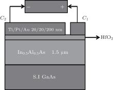
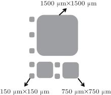
The HfO2/n– InAlAs MOS-capacitor was fabricated with the structure that is shown in Fig. 1. The 1.5-μ m n-InAlAs layer, which was Si-doped with a concentration of 1× 1011cm− 3, was deposited epitaxially on a GaAs semi-insulating substrate. The good lattice match between the two reduced the substrate influence on the capacitor. A 5-nm InAs layer was deposited on the top of the InAlAs epitaxial layer for protection, and it was subsequently removed completely by an etching process with mixed citric acid and H2O2 in 1:1 ratio for 60 s in order to adequately expose the InAlAs in preparation for HfO2 growth. The InAlAs surface was then treated with a chemical liquid containing 36%– 38% HCl to remove the native oxides. It was next treated by 7% (NH4)2S to remove elemental As and produce a good-quality InAlAs surface.[7, 8] HfO2 film was subsequently grown on the clean InAlAs epitaxially by atomic layer deposition (ALD) at 245 ° C with a pressure of 2300 Pa. A post deposition annealing (PDA) process was then used in order to form a diffusion barrier layer to prevent the interaction between HfO2 and InAlAs.[9] Considering the crystallizing points of HfO2 and InAlAs materials, the PDA temperature was chosen to be 380 ° C. Finally, Ti/Pt/Au was deposited as the metal electrode with a thickness of 20/20/200 nm, in which Pt is adopted to prevent Au from entering the semiconductor through the formation of defects and contamination. The window of the metal electrode was formed by electron-beam lithography on the top of HfO2. The layout is shown in Fig. 2. The biggest electrode is 100 times larger than the smallest one of 150× 150 μ m in order to make the C– V test accurate by using the size of electrode method.
Three kinds of HfO2/n– InAlAs MOS-capacitor samples with different oxide thickness (tox) values of 6, 8, and 10 nm were prepared by different growth circles using ALD. Figure 3 shows the XPS measurements on the HfO2 surface after PDA processing. Given that 3d is present in Fig. 3(a), it can be seen that the bulk peak of the 6-nm sample moving towards the lower binding energy side is mainly attributed to As– InAl compounds with high concentration compared with those of 8-nm and 10-nm samples, suggesting that 6 nm is thin enough to allow the InAlAs– HfO2 interfacial component to be detected. As tox is increased, the As3d peak moves towards to the higher binding energy direction, primarily due to the formation of As– H compounds induced by the surface treatment. It is worth noticing that the concentration of As element does not vary obviously as tox is increased. This implies that the As in HfO2 dielectric has a strong diffusion ability and that As could capture oxygen atoms from HfO2 to form As– O states in the oxide layer, leading to redundant vacancy oxygen to form charge traps. As shown in Fig. 3(b), In 3d5/2 is found in greatly different concentrations for the samples with different tox values. The peak is obviously detected for the 6-nm sample, which can be explained by the In– AlAs states at 444.38 eV, In2O states at 444.83 eV, and In2O3 at 445.2 eV.[10] In this case, the In– O states generate the vacancy oxygen and degrade the quality of the HfO2 surface. However, the peak value is difficult to observe for 8 nm and 10 nm samples, indicating a weak diffusivity of In element in HfO2 dielectric. Therefore, In compounds are not able to degrade the quality of oxide layers for samples with high tox values. Figure 3(c) presents the XPS result for Hf 4f. It is observed that the peak for the 6-nm sample possesses a high binding energy compared with those for the 8-nm and 10-nm samples because the 6-nm oxide layer is thin enough to detect HfAlO generated in the transition layer between HfO2 and InAlAs, whereas HfAlO cannot be detected on HfO2 surface when tox is increased to 10 nm, so an enhanced concentration of HfO2 makes the Hf 4f peak shift towards a lower binding energy. The O 1s core level spectra in Fig. 3(d) also presents the same trend as Hf 4f spectra to show the appearance of HfAlO for the 6-nm sample. As tox is increased, the enhanced concentration of HfO2 makes the bulk peak drift towards the lower binding energy side. Meanwhile, other non-ideal oxide (As– O, In– O, and Al– O states) are obviously reduced, causing a pure oxide layer surface that improves the quality of the MOS-capacitor.
An etching process is applied to HfO2 dielectric to further analyze the HfO2– InAlAs interface. In order to present the most typical distinctions for different HfO2 thickness values, only 6-nm and 10-nm samples are discussed here. The XPS measurements are shown in Fig. 4. It is found that HfAlO with a higher dielectric constant than HfO2 is detected on the interface of each of the 6-nm and 10-nm samples, which performs as a buffer layer to suppress the interaction between HfO2 and InAlAs. Meanwhile a great many of As– O states, and amounts of light for In– O and Al– O states are detected on the interface, which could degrade the interfacial performance. In particular, a higher concentration of HfO2 is detected for the 10-nm sample than that for the 6-nm sample, which is primarily attributed to the reduction of As– O states, which improves the quality of the interface and electrical performance of the MOS-capacitor.
 | Fig. 4. Interfacial oxide performances with different tox values of 6 nm and 10 nm (a) interfacial XPS spectra measurements for O1s and (b) various oxide ratios. |
The C– V test of the MOS-capacitor with different tox values at 1 MHz by using high frequency equivalent capacitance method is shown in Fig. 5. The values of the accumulated capacitor 


where A is the area of capacitor, ε SiO2 is the equivalent dielectric of SiO2 (3.9), ε 0 is the permittivity of free space, k is the Boltzmann constant, T is the thermodynamic temperature, q is the electron charge, ε InAlAs is the equivalent dielectric of InAlAs (12.42), Nd is the doping concentration of n-InAlAs, and ni is the intrinsic carrier concentration of InAlAs at room temperature (i.e., 1.35× 106 cm− 3).
 | Fig. 5. C– V characteristics and the hysteresis performances of HfO2/n– InAlAs MOS-capacitor with different tox values. |
An obvious downward bending in the C– V measurement for the 6-nm sample with a bias more than 0 V is observed to infer a very serious leakage current, which is induced by the poor quality of HfO2 film and the HfO2– InAlAs interface. In contrast, the bending could basically not be detected when tox is increased to 10 nm, implying an improved leakage current performance.
| Table 1. Electrical parameters extracted from the C– V measurements for HfO2/n– InAlAs MOS-capacitor with different tox values. |
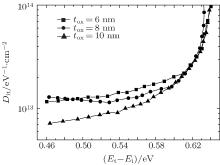
The interface traps as the centers of generation and the recombination for minority carriers effectively influence the sub-threshold swing, the threshold voltage, and the leakage current performance of the MOS-capacitor, which is greatly dependent on the match between dielectric and semiconductor.[10] Additionally, the interface trap density Dit values calculated by the Terman method from the C– V test result, [8, 12] as shown in Fig. 6, suggest that the interfacial performance is also influenced by the thickness of the oxide layer. It is shown that the 6-nm sample has the biggest Dit of 1013/eV· cm2– 1014/eV· cm2, which is primarily induced by the massive As– O states at the interface, but when tox is increased to 10 nm, Dit is improved by lower than 1013/eV· cm2 for most calculated ranges due to the enhanced ratio of HfO2 (as analysed above). However, the Dit of the 10-nm sample is still higher than that of the conventional HfO2/Si MOS-capacitor, which could be primarily explained by the poorer match between HfO2 and InAlAs. On the other hand, the PDA process could influence the interfacial characteristics, but in this paper 380 ° C is not the optimal PDA temperature[15] to most effectively suppress the interaction between HfO2 and InAlAs. Therefore, our next investigation will examine the improvement of the PDA process to further enhance the interfacial performance of the MOS-capacitor.
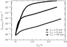
As shown in the above conclusions, the qualities of HfO2 surface and HfO2– InAlAs interface are improved as tox increases. Therefore, the leakage current of the HfO2/InAlAs MOS-capacitor should be effectively reduced by increasing the HfO2 thickness, which is verified by the I– V test result in Fig. 7. The leakage current density Jleakage for the 6-nm sample is biggest; Jleakage is reduced by two orders of magnitude as tox is increased to 8 nm; and, when tox approaches 10 nm, Jleakage achieves a very low values of 10− 7 A/cm2– 10− 5 A/cm2 under bias condition of 0 V– 2 V (i.e., the leakage current is 10− 10 A– 10− 8 A). This indicates an obvious improvement compared with the metal-semiconductor Schottky structure, which is enough for most applications of the MOS-capacitor. But if tox is continually increased to more than 10 nm, then the threshold voltage Vth may be degraded to an unacceptably high value (as discussed above) and the power dissipation could deteriorate significantly. Therefore, increasing the thickness of HfO2 layer up to 10 nm is adequate for most applications of a HfO2/InAlAs MOS-capacitor.
In this paper, HfO2/InAlAs MOS-capacitor samples with different oxide thickness tox values of 6, 8, and 10 nm are investigated. The XPS test result demonstrates that the quality of HfO2 surface is enhanced when tox is increased, while the interface trap density Dit is reduced. As a result, the leakage current of the MOS-capacitor is effectively improved by increasing tox. We achieve a significant low leakage current density of 10− 7 A/ cm2– 10− 5 A/ cm2 with gate voltage increasing from 0 V to 2 V when the HfO2 thickness is chosen to be 10 nm, which is suitable for further application to InAs/AlSb HEMTs.
| 1 |
|
| 2 |
|
| 3 |
|
| 4 |
|
| 5 |
|
| 6 |
|
| 7 |
|
| 8 |
|
| 9 |
|
| 10 |
|
| 11 |
|
| 12 |
|
| 13 |
|
| 14 |
|
| 15 |
|


