† Corresponding author. E-mail:
Project supported by the National Natural Science Foundation of China (Grant No. 61705066), the Open Fund of State Key Laboratory of Information Photonics and Optical Communications (Beijing University of Posts and Telecommunications), China (Grant No. IPOC2018B004), and the National Key Research and Development Program, China (Grant No. 2016YFA0202401).
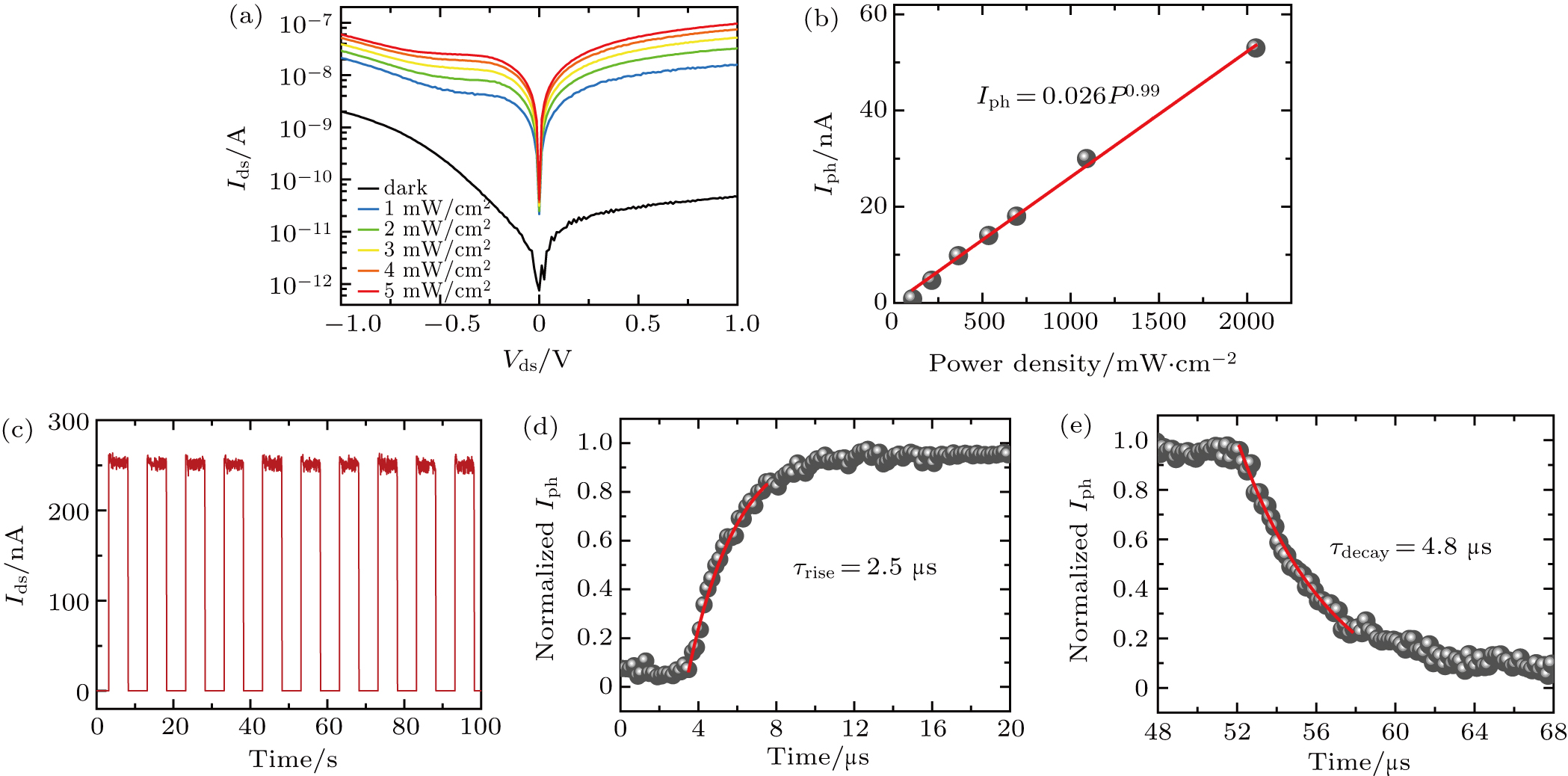
Bi2O2Se thin film could be one of the promising material candidates for the next-generation electronic and optoelectronic applications. However, the performance of Bi2O2Se thin film-based device is not fully explored in the photodetecting area. Considering the fact that the electrical properties such as carrier mobility, work function, and energy band structure of Bi2O2Se are thickness-dependent, the in-plane Bi2O2Se homojunctions consisting of layers with different thicknesses are successfully synthesized by the chemical vapor deposition (CVD) method across the terraces on the mica substrates, where terraces are created in the mica surface layer peeling off process. In this way, effective internal electrical fields are built up along the Bi2O2Se homojunctions, exhibiting diode-like rectification behavior with an on/off ratio of 102, what is more, thus obtained photodetectors possess highly sensitive and ultrafast features, with a maximum photoresponsivity of 2.5 A/W and a lifetime of 4.8 μs. Comparing with the Bi2O2Se uniform thin films, the photo-electric conversion efficiency is greatly improved for the in-plane homojunctions.
Two-dimensional (2D) layered materials with the vertical dimension limited in several atomic layers have aroused intense research interest in the next-generation electronic and optoelectronic applications.[1–4] Quantum confinement effects accompanied with the thickness shrinking lead to various unique material features including novel intrinsic physics and versatile application functionalities.[5,6] A series of functional 2D materials have been used as the transparent electrodes,[7] dielectric layers,[8] light absorbing layers,[9] and phototransistor channel materials,[10] playing a key role in the photo-detecting areas with different device architectures.
Furthermore, the vertical heterostructures based on the layer-by-layer transfer of 2D materials are attractive for realizing efficient charge transfer interfaces with the vertical electrical fields building up, which significantly improves the photo-induced electron–hole pair separation and collection processes, in this way, the overall device quantum efficiency was increased.[11,12] However, the transfer procedures for the vertical 2D heterostructures are complicated and the use of organic adhesive polymers to assist the 2D materials stacking are inevitable, which causes the device performance to be deteriorated by residual contamination. To avoid these problems, 2D in-plane junctions (IPJs) have been developed, exhibiting promising prospects for fundamental researches and device explorations.
IPJs are generally formed by direct lateral overgrowth along the edges of the existed 2D films.[13] The advantages of the IPJ structures, such as atomically sharp in-plane interface, sub-nanometer scale band alignment engineering,[14] have been increasingly received attentions and further promoted the innovations of the IPJ fabrication technique. Specifically, the in-plane 1T/2H phase modulating under the gate voltage in the thin MoS2 films created efficient Schottky junctions,[15] the selective chemical doping of MoS2 flakes fulfilled in-plane p–n junctions for the diodes fabrication,[16] what is more, alternate electric doping of WSe2 layers promotes the lateral homojunction formation to construct sensitive photodetectors.[17] These efforts have enriched the development of various IPJ structures, displaying great potentials for the future device applications.
In this work, the Bi2O2Se homogeneous IPJs consisting of two or more junctions with different layer thicknesses are reported, which then are adopted in the high-performance photodetectors with the metal/semiconductor/metal architecture. The Bi2O2Se thin film is synthesized on fluorophlogopite mica (“f-mica” for abbreviation) substrate for the first time by Peng et al. through the chemical vapor deposition (CVD) method,[18] exhibiting outstanding electrical and opto-electrical properties such as high carrier mobility,[19] narrow bandgap,[20] and ultrafast photo-response speed.[21] However, the device performance of the photodetectors based on the Bi2O2Se thin films is not fully explored. Especially, the device response speed is on the millisecond order[22] or several hundred microseconds,[23] which is much slower than the intrinsic picosecond scaled opto-electric process at the Bi2O2Se/metal interface.[21] The realization of Bi2O2Se homogeneous IPJs effectively builds up an internal lateral electric field at the IPJ interface due to the fact that the energy band structure of Bi2O2Se film is thickness-dependent,[19] which improves the photo-induced electron–hole pair dissociation efficiency. As a result, the response time of the photodetectors based on the Bi2O2Se IPJs is accelerated to 4.8 μs. Besides, the device photoresponsivity reaches 2.5 A/W and the detectivity 3.2 × 10⁸ Jones (1 Jones = 1 cm⋅Hz1/2⋅W−1). Here in this work, the layer thickness modulation in the Bi2O2Se IPJs is realized across the f-mica steps which are created manually in the process of repeated peeling off the mica surface layers. Additionally, the Bi2O2Se films with different thicknesses can merge together, thereby the Bi2O2Se homojunctions are also obtained.
Part of the surface layers on the fluorophlogopite mica substrates, KMg3(AlSi3O10)F2, were peeled away with a Scotch tape repeatedly. In this way, terraces were formed on the mica surface with a step height of about several nanometers. The Bi2O2Se IPJs with different layer thicknesses laterally were then obtained across the mica steps by the CVD epitaxial growth. The pre-treated mica substrates were placed at 10-cm downstream from the heating center where the Bi2O3 powder (purchased from Alfa Aesar, with a purity of 99.99%) was placed. The Bi2Se3 (with 99.999% purity supplied from Alfa Aesar) flakes were located at 7-cm upstream of Bi2O3. Nitrogen was used as the carrier gas and the flux was set to be 150 sccm. The pressure in the furnace was kept at 2500 Pa. The temperature of the furnace center was set to increase from room temperature (RT, 23 °C) to 580 °C in 30 min and kept at 580 °C for 60 min, then cooled down to RT naturally. The thickness and morphology of the as-grown Bi2O2Se IPJs were characterized with the Park XE7 AFM system.
The Pd/Au film with the thickness of 10 nm and 100 nm were evaporated sequentially on SiO2/Si substrates, which was patterned with the copper TEM grids acting as the shadow masks. The Pd/Au electrodes were then fulfilled on the thinner and thicker Bi2O2Se IPJs layers in a peeling up and placing down procedure assisted with a probe tip under the optical microscope. The fabricated Pd/Bi2O2Se/Pd structures were annealed in a CVD quartz tube under a pressure of 8 Pa at 200 °C with no carrier gas.
The device performance characterizations (the electrical and optoelectronic measurements) were carried out under the vacuum condition of 10−3 Torr (1 Torr = 1.33322 × 10² Pa) in a Lakeshore TTPX probe station at 27 °C (300 K). The device electrical curves were obtained with the Keysight B1500 SMUs. The photo-response experiments were performed under 640-nm laser illuminating with a 1-cm2 laser spot in diameter. The response speed of the Bi2O2Se IPJs was measured using a data acquisition card (NI PCIe-6321).
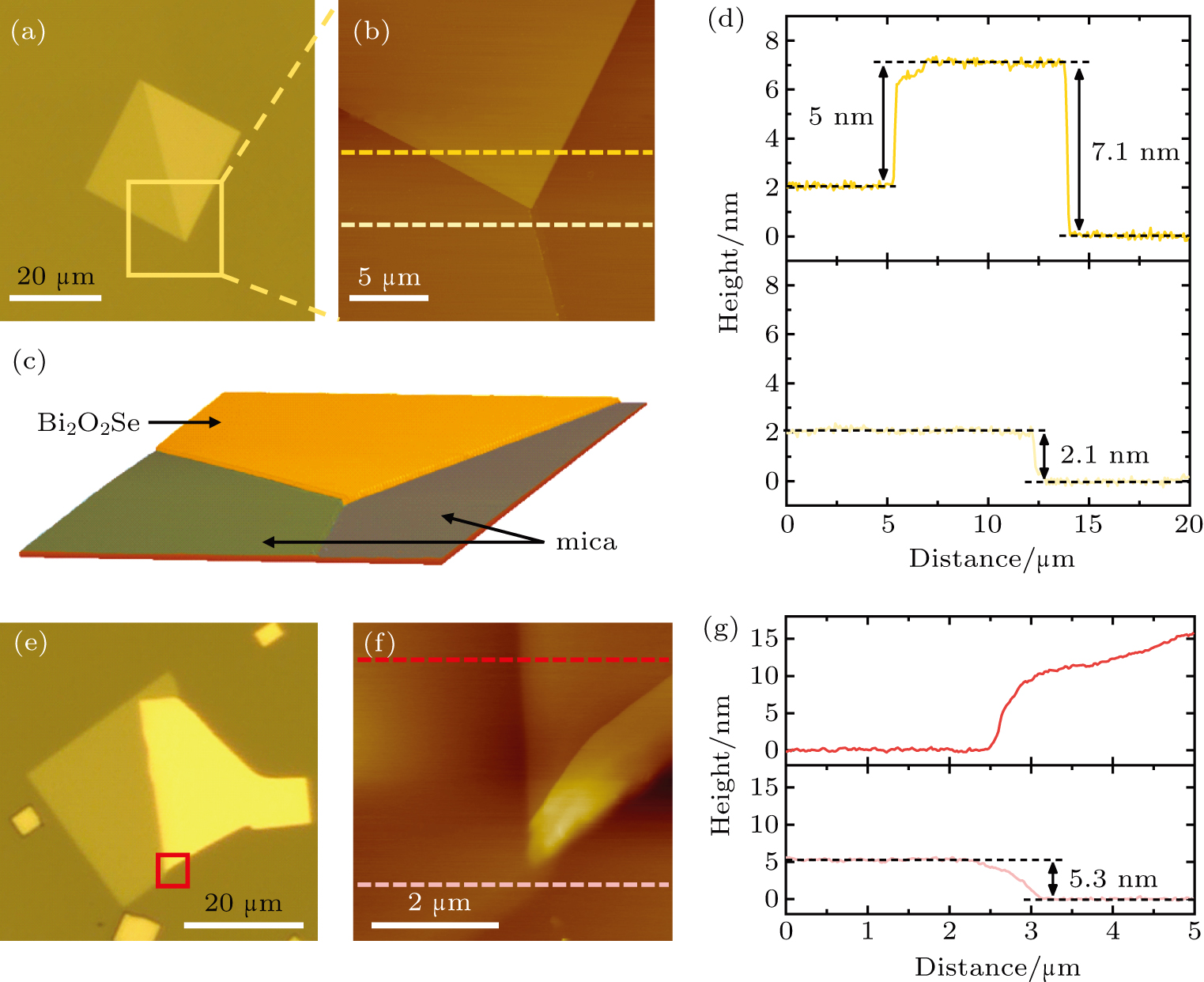
The pre-treating of the mica substrates is schematically illustrated as shown in Fig.
 | Fig. 2. The optical microscopic images of as-synthesized Bi2O2Se IPJs across mica steps showing ((a), (b)) three Bi2O2Se films affected by the same mica layer edge obviously. |
What needs mentioning is that the Bi2O2Se IPJs can be formed by more than two junctions as indicated in Fig.
With the fabricated Bi2O2Se IPJs, atomic force microscopy (AFM) analysis is performed to characterize the thickness information and the film morphologies. Figure
What is more, another case for the Bi2O2Se IPJs formation is that the nearby Bi2O2Se films are merged together. There exists obvious difference in optical contrast in the OM image of Fig.
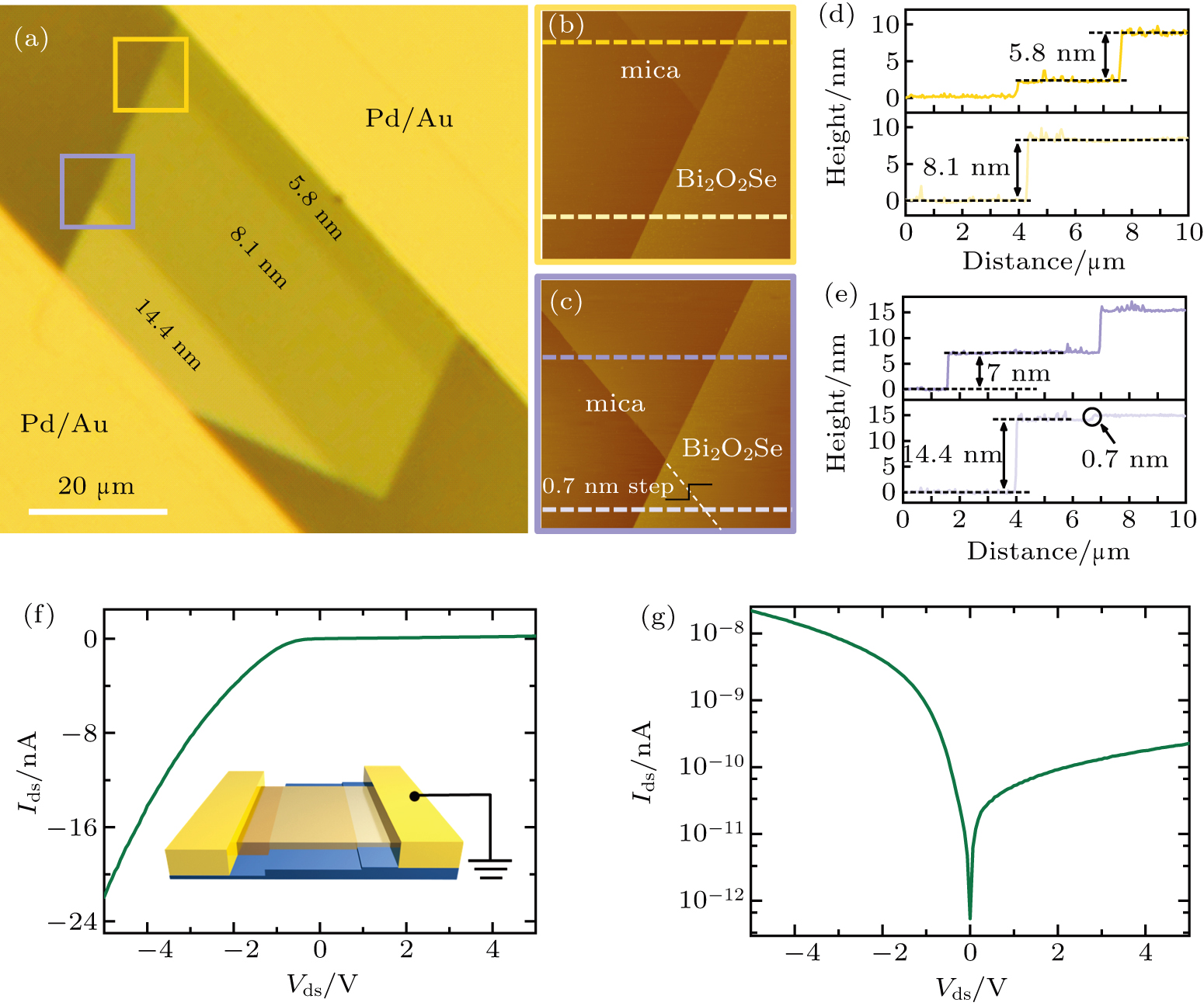
From the AFM results, the surface of the Bi2O2Se IPJ under the laminating growth is continuous without dislocations, then it is believed that the corresponding optoelectronic performance is desirable owing to the fact that the effective in-plane electrical field is built up at the IPJ interface. Based on the Bi2O2Se IPJs with three junctions of different thicknesses, efficient photodetectors are fabricated with Pd/Au (10 nm/100 nm) serving as the electrodes. The device OM image is shown in Fig.
The photoresponse performance of the photodetector based on Bi2O2Se IPJ is characterized as shown in Fig.
With the charge transfer states effectively formed at the IPJ interfaces between the Bi2O2Se layers with different thickness, the device response speed can be significantly accelerated, owing to the fact that the carrier transport routes are improved from the aspects of the light induced electron–hole pair separation, carrier drifting along the electrical fields within the IPJ, and the carrier collection by the electrodes. The Bi2O2Se IPJ photoresponse speed is measured under the 640-nm laser on-off modulation as indicated in Fig.
To further verify the improvement in photodetecting performance of the Bi2O2Se IPJ structures, reference devices based on the Bi2O2Se thin films with uniform layer thickness were fabricated also with Pd/Au as the electrodes. The device electrical performance is shown in Fig.
The Bi2O2Se in-plane junctions are successfully synthesized across the mica steps created by peeling off the mica surface layer. The Bi2O2Se IPJs are constructed by layers with different thickness, and the surface of which is flat and continuous, showing high crystal quality and laminating growth mode. Photodetectors fabricated based on the Bi2O2Se IPJs exhibit diode-like current rectification behavior and excellent photoresponse performance. Comparing with the devices based on the uniform Bi2O2Se thin films, the opto-electric conversion efficiency is improved, and the response speed is accelerated, which are attributed to the effective internal electrical field built up at the Bi2O2Se in-plane junction interface. We believe that the thickness modulating on the mica substrate can be applied to more 2D materials for realizing high-performance optoelectronic devices.
| [1] | |
| [2] | |
| [3] | |
| [4] | |
| [5] | |
| [6] | |
| [7] | |
| [8] | |
| [9] | |
| [10] | |
| [11] | |
| [12] | |
| [13] | |
| [14] | |
| [15] | |
| [16] | |
| [17] | |
| [18] | |
| [19] | |
| [20] | |
| [21] | |
| [22] | |
| [23] | |
| [24] | |
| [25] | |
| [26] | |
| [27] |


