Thickness-modulated in-plane Bi2O2Se homojunctions for ultrafast high-performance photodetectors
Project supported by the National Natural Science Foundation of China (Grant No. 61705066), the Open Fund of State Key Laboratory of Information Photonics and Optical Communications (Beijing University of Posts and Telecommunications), China (Grant No. IPOC2018B004), and the National Key Research and Development Program, China (Grant No. 2016YFA0202401).
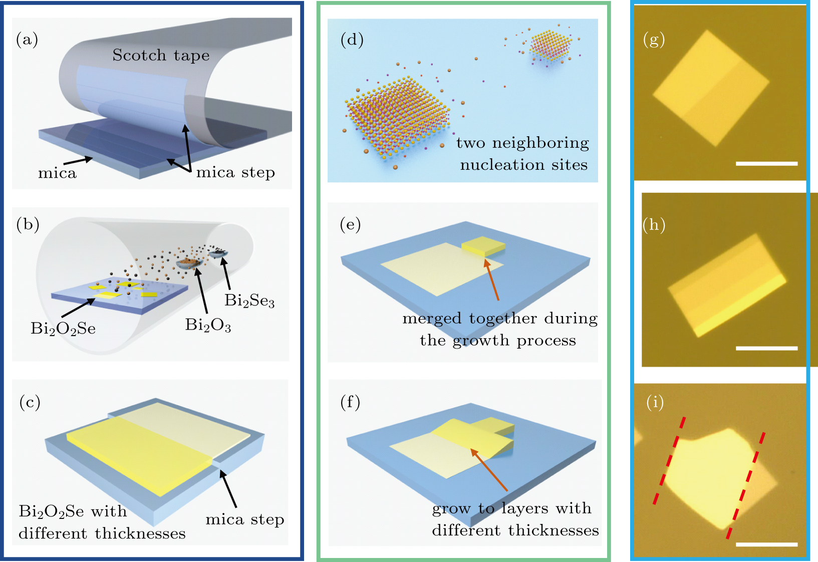
(a)–(c) Schematic illustration of Bi2O2Se homogeneous in-plane junction fabrication process with the mica substrate pre-treating, (d)–(f) Bi2O2Se in-plane junction formed by near-distance nucleation sites merging together, (g) optical microscopic image of Bi2O2Se IPJ constructed by two layers with different thicknesses, (h) Bi2O2Se IPJ consisting four layers, (i) Bi2O2Se IPJ formed by neighboring film merging together, where red dash lines represent the parallel crystal edges of thick Bi2O2Se film. All scale bars are 20 μm.