† Corresponding author. E-mail:
Project supported by the National Key Research and Development Program of China (Grant No. 2018YFB2200500), the National Natural Science Foundation of China (Grant Nos. 61675195, 61934007, and 61974170), Opened Fund of the State Key Laboratory of Integrated Optoelectronics, China (Grant No. IOSKL2018KF17), and Beijing Natural Science Foundation, China (Grant No. 4162063).
An investigation of germanium-tin (GeSn) on silicon p–i–n photodetectors with a high-quality Ge0.94Sn0.06 absorbing layer is reported. The GeSn photodetector reached a responsivity as high as 0.45 A/W at the wavelength of 1550 nm and 0.12 A/W at the wavelength of 2 μm. A cycle annealing technology was applied to improve the quality of the epitaxial layer during the growth process by molecular beam epitaxy. A low dark-current density under 1 V reverse bias about 0.078 A/cm2 was achieved at room temperature. Furthermore, the GeSn photodetector could detect a wide spectrum region and the cutoff wavelength reached to about 2.3 μm. This work has great importance in silicon-based short-wave infrared detection.
Germanium-tin alloy (GeSn), a new group IV compound, has recently attracted significant research interest due to its good performance of tunable bandgap width[1,2] and enhanced carrier mobility compared with other group IV material or compound.[3] Research shows that the increase of Sn concentration in GeSn leads to a decrease of its bandgap width. This phenomenon extends the detection zone of the GeSn photodetector toward longer wavelengths, therefore GeSn photodetector can be utilized in short-wave infrared (SWIR) applications, including infrared imagery field, non-invasive detecting, medical diagnostics, fiber-optic telecommunications, and so on.[4–8] Furthermore, the manufacturing process of GeSn alloy is compatible with Si complementary metal oxide semiconductor (CMOS) processing technology, which shows a huge potential in silicon-based optoelectronics.[9]
However, there are significant challenges in growing high-quality GeSn materials. For example, the equilibrium solubility of Sn in Ge is lower than 1%,[10] Sn easily segregates with temperature increasing, and the lattice mismatch between Ge and α-Sn is as large as 14.7%.[11,12] In order to release the misfit dislocation between the Ge buffer and Si substrate, we adopted a two-step growth method to grow the Ge buffer all the time.[13] However, it would produce plentiful threading dislocations that can spread to the upper GeSn layer and eventually damage the quality of the upper material. In this work, we adopted multiple cycle annealing to grow high-quality GeSn alloy by molecular beam epitaxy (MBE). Multiple cycle annealing minimizes the dislocation in the Ge buffer, at the same time introduces tensile strain in the epitaxial Ge buffer.[14] This tensile strain can partially relieve the compressive strain caused by large lattice mismatch in following epitaxial GeSn layer, thus optimizing the quality of the GeSn layer.
The silicon-based GeSn p–i–n photodetector was fabricated with high-quality Ge0.94Sn0.06 materials. The device exhibited well-behaved diode characteristics with a low dark-current density about 0.078 A/cm2 under 1 V reverse bias at room temperature. In addition, the spectral response of the GeSn photodetector has covered most of the SWIR wavelength, whose cutoff wavelength can reach to about 2.3 μm. High responsivities of 0.45 A/W and 0.12 A/W were achieved at the wavelengths of 1550 nm and 2 μm, respectively. As shown in Fig.
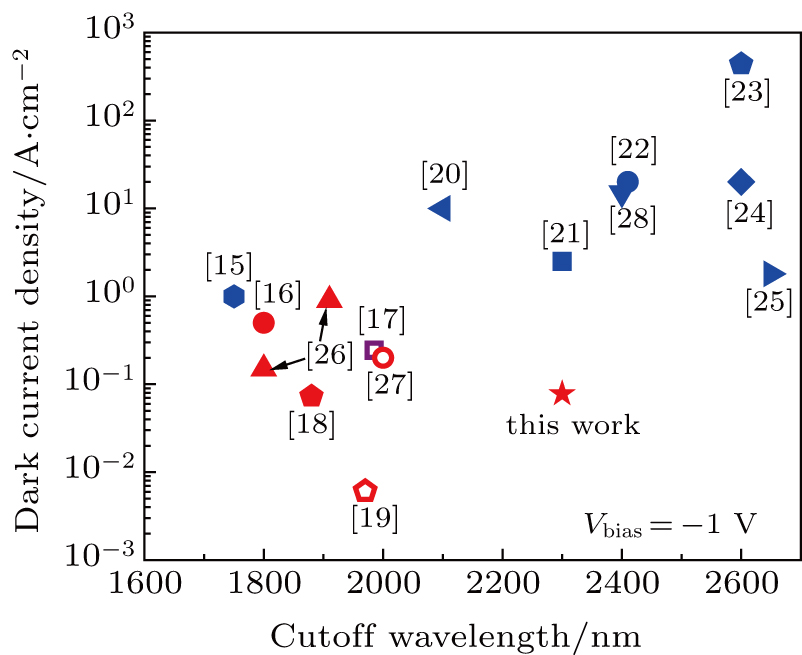 | Fig. 1. Comparison of dark current density for GeSn photodetectors at a reverse bias of 1 V in different groups.[15–28] Different colors of the icons represent the different growth methods of GeSn alloy, red, purple, and blue refer to the growth methods of MBE, magnetron sputtering epitaxy, and CVD, respectively. Solid or hollow icons refer to the GeSn materials grown on Si substrate or on Ge substrate, on which devices were fabricated. |
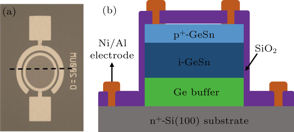
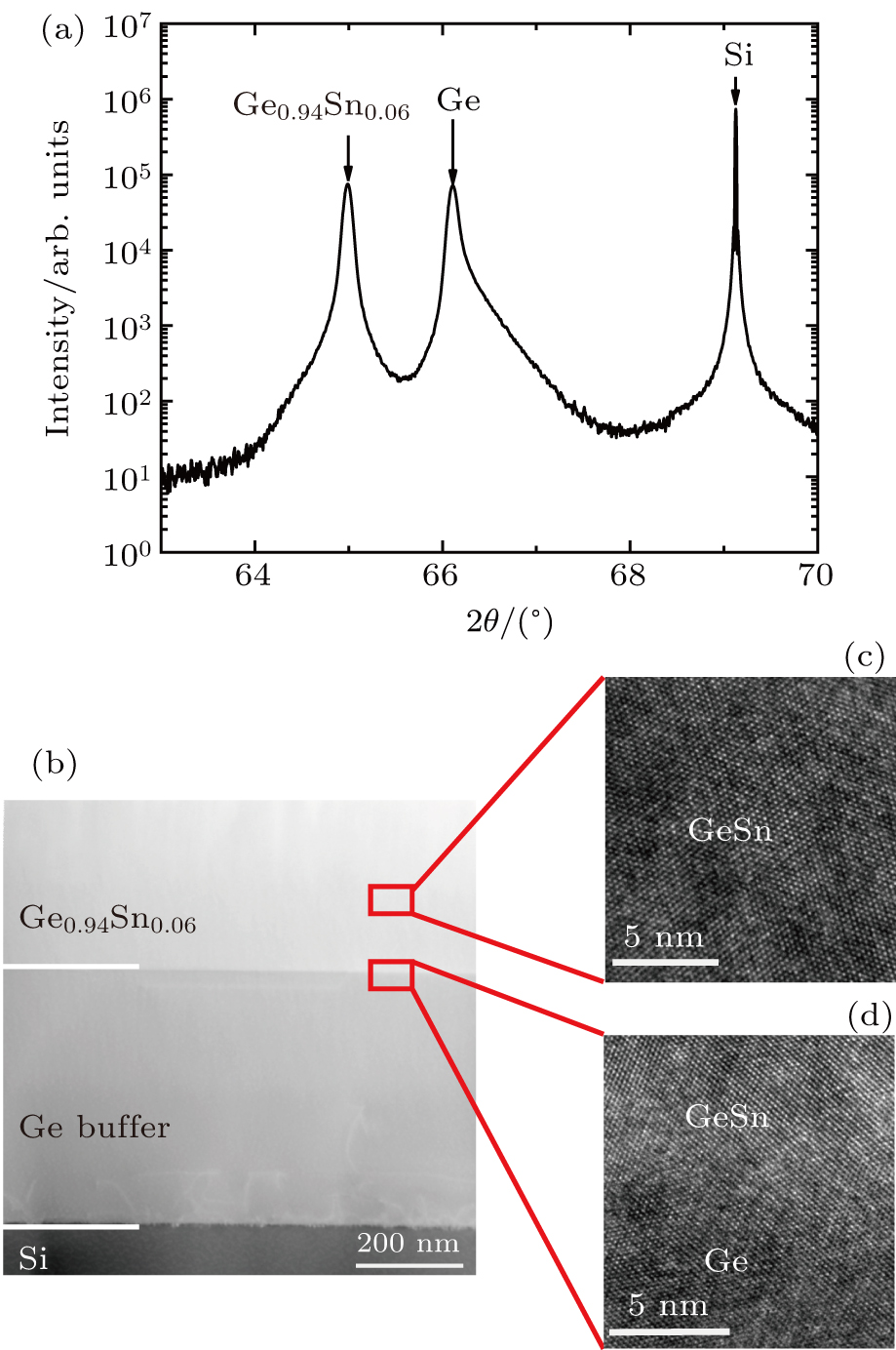
The material was grown on n-type Si (100) substrate with solid source molecular beam epitaxy. The epitaxial layer stacks consist of a 500 nm-thick Ge buffer, and a 650 nm-thick Ge0.94Sn0.06 absorbing layer grown at 180 °C. The Ge buffer was grown by a two-step growth method, composed by 100 nm-thick low temperature Ge (LT-Ge) and 400 nm-thick high temperature Ge (HT-Ge), and underwent a multiple-cycle annealing from 600 °C to 800 °C, which was designed to improve the quality of the Ge and GeSn layers. Owing to significant challenges mentioned above, growing high-quality GeSn material directly on Si substrate is difficult. Currently, we always use the high–low temperature growth method (known as two-step growth method) to grow the Ge buffer. This method can release partial misfit dislocations at the Si and Ge interface. Meanwhile, it produces plentiful threading dislocations, which will spread to the upper GeSn material and decrease the material quality. It has been proved that multiple-cycle annealing can minimize the dislocation in the Ge buffer.[14] High temperature (as close as possible, but not higher than the melting point of Ge) provides energy to the dislocations which exist in the epitaxial film, makes them migrate and ultimately quench. Furthermore, considering the different thermal expansion coefficients between Ge and Si, the epitaxial Ge buffer will induce tensile strain in cycle annealing, as shown in Table
To form p+ Ge0.94Sn0.06 contact, the top of the GeSn layer was implanted by boron fluoride ions (BF2+) with energy of 20 keV (calculated doping depth is 50 nm) and dose of 4.0 × 1015 cm−2. In order to repair the lattice damage caused by the implantation of BF2+ ions and thermally activate BF2+ ions, the material was subsequently annealed at 450 °C for 30 s in an N2 atmosphere. There is a temperature tradeoff between effectively lattice repairing and preventing Sn segregation. This sample was made out of circular mesas by standard photolithography and Cl-based inductively coupled plasma (ICP) etching with Cl2, BCl3, Ar plasma at flow rates of 10 sccm, 30 sccm, 20 sccm respectively, and 60 W RF power. These conditions realized an etch rate of 350 nm/min and produced well-defined mesas with sharp sidewalls, and smooth, residue-free surfaces.
To reduce the reflection and passivate surface of the material, a 500 nm-thick SiO2 layer was deposited on the material by plasma-enhanced chemical vapor deposition (PECVD). The electrodes were deposited on both top-GeSn layer and Si substrate using electron beam evaporation and then fabricated by a lift-off process, including a 40 nm-thick Ni adhesion layer and a 500 nm-thick Al. Through processing mentioned above, we fabricated different mesa size devices, varying from 30 μm to 200 μm. The top-view microscopic image of the Ge0.94Sn0.06 photodetector with a 200 μm-diameter mesa is shown in Fig.
The x-ray diffraction (XRD) ω–2θ scanning of the Gegji0.94Sn0.06 sample grown on Ge buffered Si(100) substrate around (004) orientation is presented in Fig.
| Table 1. Summary of lattice constant, in-plane strain, and Sn concentration. . |
The high resolution transmission electron microscopy (HR-TEM) image of the Ge0.94Sn0.06 on Ge buffered Si is shown in Fig.
In this work, we have adopted a series of instruments to measure the I–V characteristics, optical response, and spectral response of the Ge0.94Sn0.06 p–i–n photodetectors at room temperature respectively, such as Agilent B1500A semiconductor device analyzer, tunable laser (1500–1630 nm), 2000 nm laser, and Nicolet 6700 Fourier transform infrared (FTIR) spectrometer. In addition, a commercial InGaAs photodetector was measured to calibrate the spectral response.
The dark current–voltage (I–V) characteristics of the fabricated silicon-based Ge0.94Sn0.06 p–i–n photodetectors with different mesa sizes in diameter are shown in Fig.
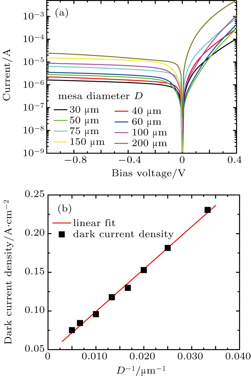 | Fig. 4. (a) The Idark–Vbias characteristics of GeSn photodetectors with various mesa sizes. (b) Dark-current density (Jdark) versus 1/D under 1 V reverse bias. |
Further analysis of the dark current density (Jdark) has been conducted, which can be expressed as
 |
According to this formula, the Jdark versus 1/D for the GeSn photodetectors at a reverse bias of 1 V bias, where D varies from 30 μm to 200 μm, is depicted in Fig.
In addition, the main source of Jsurf is interface traps around the mesa sidewall, which can introduce energy levels in the forbidden gap and eventually increase the peripheral surface leakage current. These traps were formed in the ICP etching process of the mesa. Currently, it has been reported that the passivation technique can effectively decrease the dark current, for example, forming Si,[18] yttrium-doped GeO2,[32] or GeOx/GeSnOx (formed by ozone oxidation)[33] passivation layer.
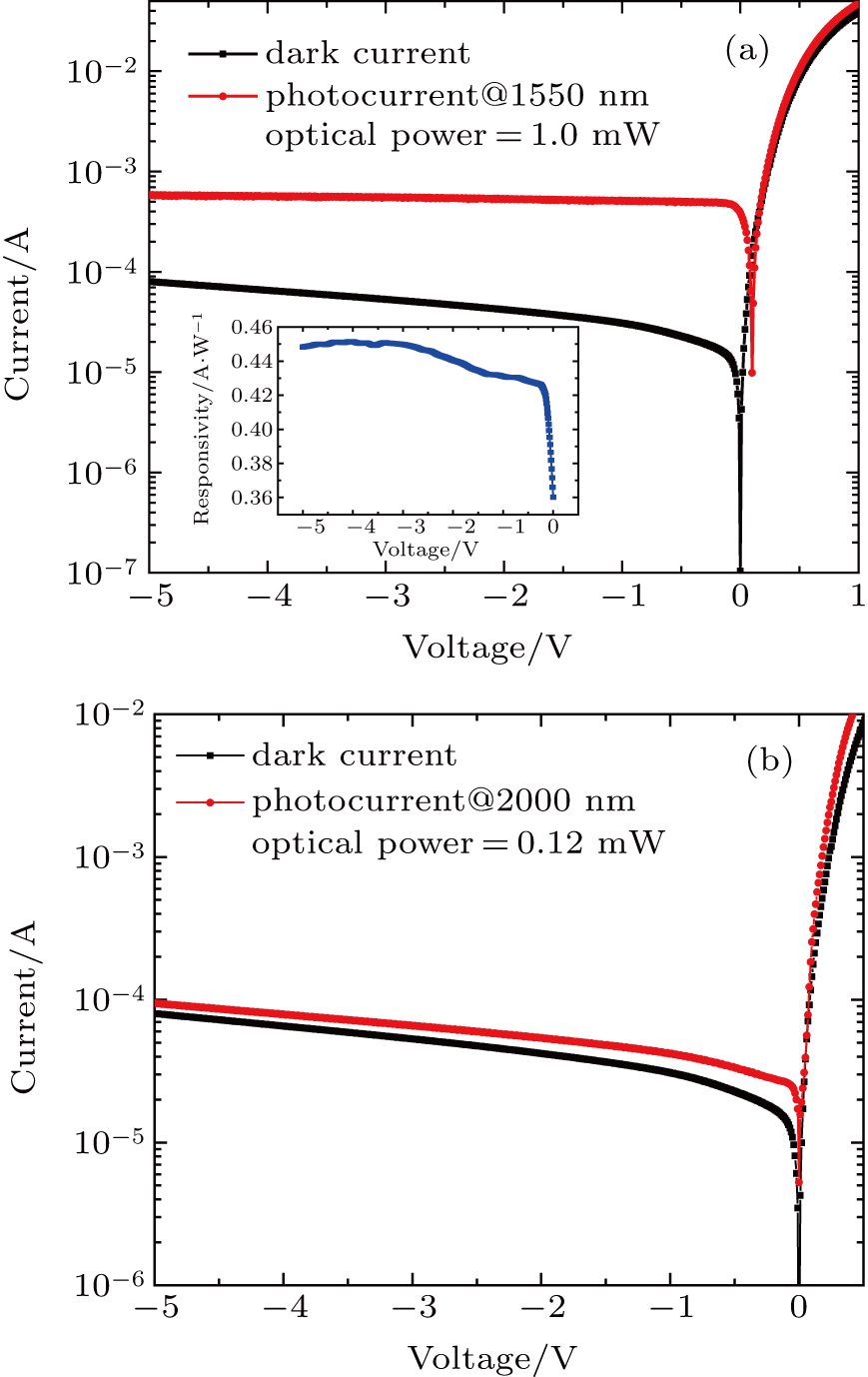
Figure
The inset displays the responsivity of the devices as a function of the applied voltage at 1550 nm. We find that photon-generated carriers are efficiently collected under a reverse bias of 0.25 V. With the increase of the reverse bias voltage, the responsivity increases slowly, finally peaks at −4.22 V. As the voltage increases further, there is a modest decline in the responsivity. This phenomenon may be caused by drastically increasing leakage current under higher reverse bias voltage. What is more, it has been reported that the Franz–Keldysh effect, which refers to the absorption coefficient dependence on the voltage, could affect the responsivity.[36]
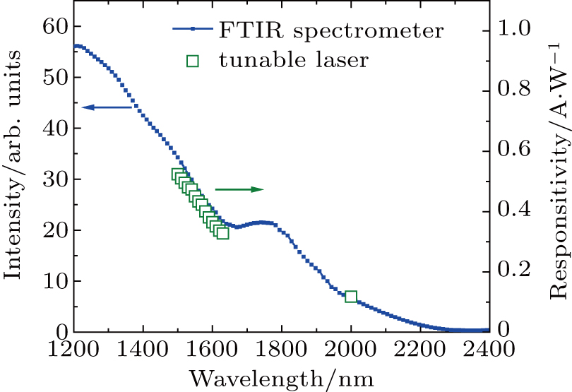
The optical spectral response (1100–2500 nm) of the GeSn photodetector is shown in Fig.
In summary, the high-quality GeSn layer was grown by MBE combined with multiple cycle annealing technology and fabricated into the silicon-based Ge0.94Sn0.06 p–i–n photodetectors adopting a CMOS compatible manufacturing process. This GeSn photodetector achieved a responsivity as high as 0.45 A/W at 1550 nm and 0.12 A/W at 2 μm. The wide spectrum detection with cutoff wavelength of 2.3 μm and dark-current density as low as 0.078 A/cm2 under a bias of −1 V were achieved. This work shows a prospective method to fabricate GeSn p–i–n photodetectors and has great importance in silicon-based short-wave infrared detection and developing cost-effective monolithically integrated Si photonics.
| [1] | |
| [2] | |
| [3] | |
| [4] | |
| [5] | |
| [6] | |
| [7] | |
| [8] | |
| [9] | |
| [10] | |
| [11] | |
| [12] | |
| [13] | |
| [14] | |
| [15] | |
| [16] | |
| [17] | |
| [18] | |
| [19] | |
| [20] | |
| [21] | |
| [22] | |
| [23] | |
| [24] | |
| [25] | |
| [26] | |
| [27] | |
| [28] | |
| [29] | |
| [30] | |
| [31] | |
| [32] | |
| [33] | |
| [34] | |
| [35] | |
| [36] |


