High performance silicon-based GeSn p–i–n photodetectors for short-wave infrared application
Project supported by the National Key Research and Development Program of China (Grant No. 2018YFB2200500), the National Natural Science Foundation of China (Grant Nos. 61675195, 61934007, and 61974170), Opened Fund of the State Key Laboratory of Integrated Optoelectronics, China (Grant No. IOSKL2018KF17), and Beijing Natural Science Foundation, China (Grant No. 4162063).
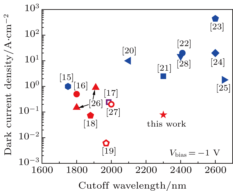
Comparison of dark current density for GeSn photodetectors at a reverse bias of 1 V in different groups.[
