High performance silicon-based GeSn p–i–n photodetectors for short-wave infrared application
Project supported by the National Key Research and Development Program of China (Grant No. 2018YFB2200500), the National Natural Science Foundation of China (Grant Nos. 61675195, 61934007, and 61974170), Opened Fund of the State Key Laboratory of Integrated Optoelectronics, China (Grant No. IOSKL2018KF17), and Beijing Natural Science Foundation, China (Grant No. 4162063).
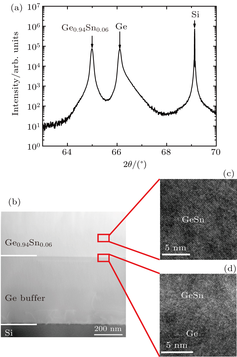
HR-XRD ω–2θ scanning of the Ge0.094Sn0.06 sample grown on Ge buffered Si(100) substrate at (004) orientation. (b) TEM image of the Ge0.94Sn0.06 sample (the white lines in the image represent the interfaces of Ge0.94Sn0.06/Ge buffer and Ge buffer/Si, respectively). (c) HR-TEM image of the Ge0.94Sn0.06 layer. (d) HR-TEM image of the interface between GeSn layer and Ge buffer layer.
