Analysis of non-uniform hetero-gate-dielectric dual-material control gate TFET for suppressing ambipolar nature and improving radio-frequency performance
Xu Hui-Fang, Cui Jian, Sun Wen, Han Xin-Feng
Institute of Electrical and Electronic Engineering, Anhui Science and Technology University, Fengyang 233100, China


† Corresponding author. E-mail: xu0342@163.com

Abstract

A tunnel field-effect transistor (TFET) is proposed by combining various advantages together, such as non-uniform gate–oxide layer, hetero-gate-dielectric (HGD), and dual-material control-gate (DMCG) technology. The effects of the length of non-uniform gate–oxide layer and dual-material control-gate on the on-state, off-state, and ambipolar currents are investigated. In addition, radio-frequency performance is studied in terms of gain bandwidth product, cut-off frequency, transit time, and transconductance frequency product. Moreover, the length of non-uniform gate–oxide layer and dual-material control-gate are optimized to improve the on-off current ratio and radio-frequency performances as well as the suppression of ambipolar current. All results demonstrate that the proposed device not only suppresses ambipolar current but also improves radio-frequency performance compared with the conventional DMCG TFET, which makes the proposed device a better application prospect in the advanced integrated circuits.

1. Introduction

In order to be better applied to integrated circuits, reduce the cost, and improve the on-state current (Ion) and high-frequency characteristics, the size of device needs to be reduced continuously. However, downscaling of the device leads to the increased power dissipation in electronic circuits because of increased leakage current in the off-state. As far as the traditional metal–oxide–semiconductor field-effect transistor (MOSFET) is concerned, it is very difficult to reduce the supply voltage for the purpose of preventing power from dissipating due to the minimum achievable thermionic emission limit of the subthreshold swing (SS) (SS=60 mV/decade) and large off-state current (Ioff). The appearance of tunnel field-effect transistor (TFET) is consistent with the trend of the continuous downsizing of devices for future ultralow power dissipation integrated circuit applications. The TFET can achieve an SS value less than 60 mV/decade at room temperature due to the fact that the carrier injection of the device from source region to channel region is based on band-to-band tunneling (BTBT).[1] Moreover, the TFET can offer other advantages such as low Ioff when the barrier width at the source-channel junction is very large in the off-state,[24] high immunity against short-channel effects (SCEs), and small supply voltage below 0.5 V.[5,6] However, the TFET has some shortcomings such as low Ion, ambipolar current (Iamb), and large Miller capacitance. The Ion should be enhanced and ambipolar behavior and Miller capacitance should be well reduced in order to make TFET a better application prospect in the future integrated circuit. Therefore, researchers should comprehensively carry forward the advantages of TFET and overcome its shortcomings. Up to now, many techniques have been proposed to improve Ion, such as narrow bandgap materials,[711] high-k gate dielectric,[12] hetero-junction mechanism,[13,14] and doping-less TFETs,[15] source-side pocket doping,[16] hetero-stacked TFET,[17] heteromaterial gate,[18,19] etc. The Iamb can be reduced by using the dual-material control-gate (DMCG) TFETs,[20] charge plasma-based TFETs with gate engineering,[21,22] gate material workfunction engineering,[23] lightly doped drain,[24] and gate–drain underlap structure.[25,26] Moreover, a hetero-gate-dielectric (HGD) TFET with a high gate–oxide dielectric near the source side and a low gate–oxide dielectric near the drain side can enhance Ion and obtain promising radio frequency performance.[2729]

The downscaling of gate–oxide layer thickness is an important method to enhance the steep switching characteristics of TFETs. But it also leads to large gate leakage current. Moreover, the thickness of the gate–oxide layer is assumed to be uniform in almost all existing TFET devices. Therefore, it is necessary to study the variation of the TFET characteristics in the case of non-uniform gate–oxide layer thickness. The non-uniform structure is defined as a structure whose gate–oxide thickness is thinner on the source-channel side while larger gate–oxide thickness on the drain-channel side. Recently, a TFET with non-uniform gate–oxide shape and an asymmetric hetero-dielectric engineered dual-material double gate (DG) TFET has been analyzed.[30,31] In the present work, a novel device is proposed by combining various advantages together such as non-uniform gate–oxide shape, HGD and DMCG, and named NDMCG TFET. It is intended that in the proposed device the Iamb value can be reduced, the on-off current ratio can be enhanced, and the radio-frequency (RF) performance can be improved by optimizing the structural parameters of device.

2. Device structure

The structure of NDMCG TFET is shown in Fig. 1. The gates closer to the source and the drain are denoted as G (tunneling gate) and G2 (auxiliary gate), respectively. The gate between G and G2 is marked as G1 (control gate). In the proposed device, the work function of G is selected to be the same as that of G2, but their work functions are less than that of G1. The parameters used in the following simulations are P+ source, channel, and N+ drain, and they are doped with concentration 1020 cm−3, 1016 cm−3, and 5×1019 cm−3, respectively. The thickness of silicon (tsi) is 10 nm, the thickness of HfO2 (t1) and the maximum thickness of SiO2 (t2) are 1 nm and 3 nm, respectively. The length of P+ source (Ls), channel (Lch), and N+ drain (Ld) are 50 nm, 50 nm, and 50 nm, respectively. The length of HfO2, G, G1, and G2 are Lox, L1, L2, and L3, respectively.

Fig. 1. Structure of non-uniform gate–oxide layer hetero-gate-dielectric DMCG TFET.

The simulations are performed by using silvaco atlas simulator,[32] and the models such as dynamic nonlocal band-to-band tunneling model, Shockley–Read–Hall model, auger recombination model, bandgap narrowing model, and Fermi statistics model are used in this work. The dynamic nonlocal band-to-band tunneling model is an important model in describing the operating principle of TFET. Using the Kane model,[33] the band-to-band tunneling generation rate is expressed as[34]

where A and B are the tunneling parameters, which are and 1.9×10⁷ V/cm, respectively;[32] E is the lateral electrical field; D is a material-dependent constant, which is 2 and 2.5 for the direct and indirect band-gap materials, respectively. The values of Ion, Ioff, and Iamb defined at Vgs=0.8 V, 0 V, and −0.5 V respectively are calculated when Vds is fixed at 0.5 V, here Vgs and Vds are the gate–source voltage and drain–source voltage, respectively.

3. Results and discussions
3.1. Performance comparison between NDMCG TFET and DMCG TFET

Figure 2 shows the energy band, carrier concentration, and electric field for two devices under thermal equilibrium state. From Fig. 2(a), it can be found that there is no change of the tunneling distance at the source/channel interface since the modification is made on the channel close to the drain side. However, the increased tunneling barrier at the drain/channel junction can be seen for the NDMCG TFET. The NDMCG TFET provides higher hole concentration and lower electron concentration than the DMCG TFET as shown in Fig. 2(b). Hence, the electric field varies at the drain/channel junction along the lateral direction between NDMCG TFET and DMCG TFET as shown in Fig. 2(c). The reduced electric field can be observed for the NDMCG TFET due to the varying band levels and the different carrier concentrations.

Fig. 2. Comparisons of curves of (a) energy band, (b) carrier concentration, and (c) electric field versus X pointion between NDMCG TFET and DMCG TFET under thermal equilibrium state.

Figure 3 shows the energy bands under ambipolar state, transfer characteristics, and SS for two devices. It can be seen that the tunneling width of NDMCG TFET is larger than that of the DMCG TFET at the drain/channel junction under ambipolar state, which can limit the number of holes to tunnel from the drain to the channel. Therefore, the NDMCG TFET can reduce the ambipolar current as depicted in Fig. 3(b). The SS as a function of Ids is shown in Fig. 3(c). It can be seen that the extracted SS behavior appears relatively gradual lasting nearly 4 orders of magnitude of drain current variation. But it is worth noting that the two devices show little difference in SS. This is mainly due to the fact that the non-uniform gate–oxide shape of NDMCG TFET is made on the channel close to the drain side, so it has little effect on the increament as well as on the drain current increament with Vgs increasing.

Fig. 3. Comparisons (a) energy band under ambipolar state, (b) transfer characteristics, and (c) subthreshold swing between NDMCG TFET and DMCG TFET.
3.2. Optimization of L1, L2, and Lox for NDMCG TFET

This subsection is dedicated to the study of the influence of variation in L2 on Ion and Ioff for NDMCG TFET as depicted in Fig. 4(a). In this case, L1 is fixed at 15 nm. The increase in L2 leads to the reduction of Ion when the length of L2 is larger than 5 nm. Moreover, the NDMCG TFET can generate optimum results of Ioff and Ion when L2 is fixed at 10 nm. The Iamb for NDMCG TFET is less than that for the DMCG TFET because the tunneling width of NDMCG TFET is larger than that of the DMCG TFET at the drain/channel junction, hence tunneling of carriers from drain to channel is reduced, resulting in reduced Iamb as shown in Fig. 4(b). Therefore, we can conclude that the proposed device provides a decent amount of suppression in Iamb and large on-off current ratio when L1, L2, and L3 are 15, 10, and 25 nm, respectively.

Fig. 4. (a) Ion and Ioff varying with L2 for NDMCG TFET, and (b) Iamb varying with L2 for NDMCG TFET and DMCG TFET.

Figure 5(a) is dedicated to the study of the influence of variation in L1 on Ion and Ioff for NDMCG TFET. In this case, L3 is fixed at 15 nm. The NDMCG TFET can generate a large on-off current ratio when L1 is 15 nm. However, Iamb for NDMCG TFET is not significantly degraded with variation in L1 since the energy band at the drain/channel junction hardly changes under these conditions as indicated in Fig. 5(b). The Iamb for NDMCG TFET is less than that for DMCG TFET, which is due to the fact that the tunneling width of NDMCG TFET is larger than that of the DMCG TFET at the drain/channel junction. Hence, we can infer that selecting L1 = 15 nm along with L2 = 20 nm and L3 = 15 nm provides a decent amount of suppression in Iamb and large on-off current ratio. Based on the preceding analysis, it is clear that the optimized dual-material control-gate lengths (L1, L2, L3) are 15, 10, 25 nm and 15, 20, 15 nm in terms of suppression in Iamb and large on-off current ratio.

Fig. 5. (a) Ion and Ioff varying with L1 for NDMCG TFET, and (b) Iamb varying with L1 for NDMCG TFET and DMCG TFET.

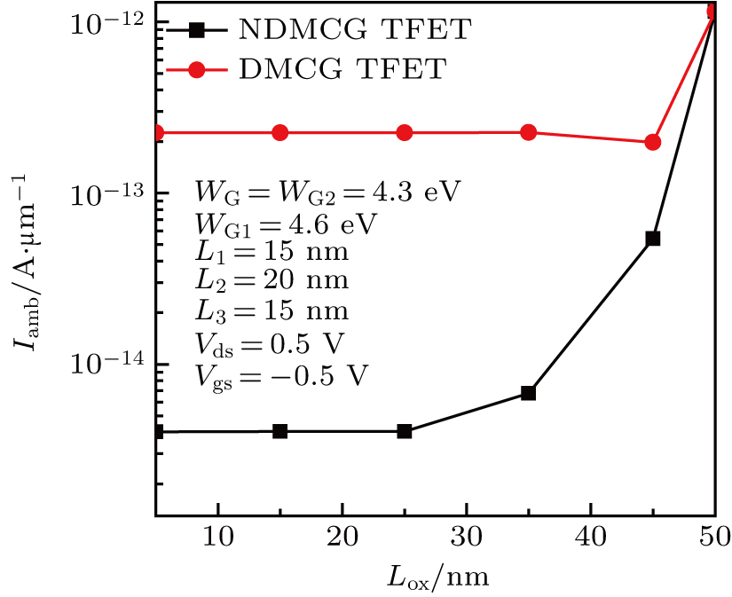
Figure 6 shows the influence of variation in Lox on Iamb for NDMCG TFET and DMCG TFET when L1, L2, and L3 are fixed at 15, 20, and 15 nm, respectively. It is expected that as Iamb increases the Lox increases because the gate control is strengthened. Moreover, when the length of Lox is longer than 35 nm, Iamb is increased sharply. It should be noted that the length of Lox is 50 nm, which represents the uniform HfO2 case (t1=t2=1 nm). The proposed device can generate small Iamb especially when Lox is less than 35 nm. Generally speaking, suppression in Iamb and large on-off current ratio can be obtained by optimizing L1, L2, L3, and Lox for the NDMCG TFET, but the optimized device has not achieved superior performance about SS compared with the DMCG TFET. However, a hetero-stacked TFET with stacked source configuration can effectively suppress the SS degradation behavior and obtain a steeper average SS by self-adaptive current replenishing with bandgap engineering.[17,35] The optimization of SS for the NDMCG TFET is not considered and it will be dealt with in our subsequent work.

Fig. 6. Iamb varying with Lox for NDMCG TFET and DMCG TFET.
3.3. Parasitic capacitance and radio-frequency performance for NDMCG TFET

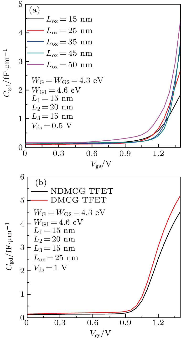
This subsection is dedicated to the study of the influence of variation in L3, and L1 on the gate–drain capacitance (Cgd) of NDMCG TFET as depicted in Fig. 7. The increase in Cgd with Vgs is due to the formation of an inversion layer in the channel region from the drain to the source. Moreover, Cgd is dominated by the inversion capacitance in the on-state. The increase of L3 in Fig. 7(a) or L1 in Fig. 7(b) represents the decrease of L2 in the proposed device. Therefore, the effect of control gate’s work function on the threshold voltage of the device becomes smaller with L2 decreasing. The threshold voltage of the proposed device decreases, which leads to an increase in charge and ultimately an increase in capacitance.

Fig. 7. Cgd varying with (a) L3 and (b) L1 for NDMCG TFET.

Figure 8(a) shows the variation of Cgd with Vgs for NDMCG TFET with L1, L2, and L3 being 15, 20, and 15 nm, respectively. It can be found that Cgd increases with Lox increasing, which is due to the fact that the gate–oxide thickness near the drain region is varied. This effect indicates the importance of the design of non-uniform gate–oxide layer. Moreover, non-uniform gate–oxide layer can reduce the coupling between the gate and the drain regions, thereby reducing Cgd. The Cgd of NDMCG TFET is less than that of DMCG TFET under all the same conditions as shown in Fig. 8(b). Therefore, The NDMCG TFET can better control the gate over the channel region.

Fig. 8. (a) CgdVgs curves for NDMCG TFET with different values of Lox, and (b) comparison of CgdVgs curve between NDMCG TFET and DMCG TFET.

Further, RF parameters of gain bandwidth product (GBP), cut-off frequency (ft), transit time (τ), and transconductance frequency product (TFP) are analyzed. The GBP determines the maximum working frequency for a direct current gain of 10, and the formula of GBP is ,[15,22] where gm is the transconductance. ft is the frequency at which the short-circuit current gain is unity, a criterion that is important for the quantification of the TFET performance in high-speed digital applications. The ft is defined as ,[15,22] where Cgs is the gate–source capacitance. Figures 9(a) and 9(b) show that the NDMCG TFET with 10 nm of L3 exhibits high GBP and ft due to the reduced parasitic capacitance and enhanced transconductance. Similarly, the NDMCG TFET with 15 nm of L1 exhibits high GBP and ft as shown in Figs. 10(a) and 10(b).

Fig. 9. Curves of (a) GBP, (b) ft, (c) τ, and (d) TFP versus Vgs of NDMCG TFET for different values of L3.

Transit time (τ) is defined as the time taken for carriers to flow from source to drain region, and it is also another important parameter to confirm the NDMCG TFET for high-frequency operation, which is expressed as . The comparison of τ between NDMCG TFETs with different values of L3 (Fig. 9(c)) and L1 (Fig. 10(c)) explains that the values of τ for NDMCG TFET under the lengths of L1, L2, L3 being respectively 15, 25, 10 nm and 15, 20, 15 nm are less than those in the other cases over the entire range of Vgs. Therefore, better response and high operational speed can be obtained in both cases. Transconductance frequency product (TFP) is another important parameter to obtain the device characteristics for high-speed designs, and it is defined as , where Ids is the drain–source current. The comparative results of the TFP for the proposed device are shown in Figs. 9(d) and 10(d), respectively. It can be found that the TFP of the proposed device reaches a peak value. However, the value begins to decrease as Vgs increases due to mobility degradation. Combining the analysis results of suppression in Iamb and large on-off current ratio, the optimized dual-material control-gate lengths of L1, L2, and L3 are obtained to be 15, 20, 15 nm, respectively.

Fig. 10. Curves of (a) GBP, (b) ft, (c) τ, and (d) TFP versus Vgs for NDMCG TFET with different values of L1.

Figure 11 shows the influences of variation in Lox on GBP, ft, τ, and TFP for NDMCG TFET, with L1, L2, and L3 fixed at 15, 20, and 15 nm, respectively. It can be found that the maximum values of GBP, ft, and TFP increase with the value of Lox increasing, but the values of three parameters described above decrease when the length of Lox is 50 nm. It should be noted that the length of Lox is 50 nm, which represents the uniform HfO2 case (t1=t2=1 nm). The proposed device embodies the advantages of non-uniform hetero-gate-dielectric in terms of three parameters, and an optimum value (Lox=45 nm) exists at which the parameters are maximum. It is worth noting that there is little difference among the three parameters when Lox is 45 nm and 35 nm, separately. By combining with the analysis results of Fig. 6, the optimum value of Lox is obtained to be 35 nm. But the difference in transit time is not obvious in the above cases.

Fig. 11. Curves of (a) GBP, (b) ft, (c) τ, and (d) TFP versus Vgs for NDMCG TFET with different values of Lox.

Figure 12 shows comparison of curves of GBP, ft, τ, and TFP versus Vgs between NDMCG TFET and DMCG TFET, with Lox, L1, L2, and L3 fixed at 35, 15, 20, and 15 nm, respectively. The results show that the NDMCG TFET has a better RF performance than the conventional DMCG TFET. High GBP implies larger gain as well as bandwidth, the increase in ft results in small switching delay. All these results demonstrate that the proposed device has a better prospect of high-speed and high-frequency applications in the advanced integrated circuits.

Fig. 12. Comparison of curves of (a) GBP, (b) ft, τ, and (c) TFP versus Vgs between NDMCG TFET and DMCG TFET, with Vds fixed at 1 V.

The above-mentioned parasitic capacitance and RF parameters for TFETs are analyzed when Vds is 1 V, and the maximum values for GBP, ft, and TFP are achieved when Vgs is nearly 1.1 V. However, according to the projection of International Technology Roadmap for Semiconductor (ITRS), the TFET has a great potential for low-power applications. In this case, Vds is lower than 1 V. Therefore, the device optimization is also analyzed when Vds is fixed at 0.5 V as indicated in Fig. 13, from which we can infer that the NDMCG TFET enhances the RF parameters compared with the conventional DMCG TFET under lower power supply voltage. Moreover, the maximum values for GBP, ft, and TFP are achieved when Vgs is nearly 0.7 V. Therefore, the proposed device is also suitable for power supply voltage applications.

Fig. 13. Comparison of curves of (a) GBP, (b) ft, τ, and (c) TFP versus Vgs between NDMCG TFET and DMCG TFET, with Vds fixed at 0.5 V.
4. Conclusions

The performances of NDMCG TFET are studied based on TCAD simulations. We demonstrate that the increase of Lox affects Iamb, but has little effect on Ion and Ioff. The results show that the design of a non-uniform gate–oxide layer with Lox being 35 nm and the dual-material control-gate lengths L1, L2, and L3 being respectively 15, 20, 15 nm can realize high Ion/Ioff and RF parameters with relatively low value of Iamb. When the drain–source voltage is fixed at 1 V for the optimized device, the RF parameters GBP, ft, and TFP are investigated, of which the maximum values are 199 GHz, 1.2 THz, and 6.1 THz, respectively. Moreover, the RF parameters of the NDMCG TFET are enhanced compared with those of the conventional DMCG TFET under lower power supply voltage. The results indicate that the NDMCG TFET has the great potential applications in high-performance RF component, which should be the superiority in future high-frequency, and high-switching-speed electronics applications.

Reference
1 Guan Y H Li Z C Luo D X Meng Q Z Zhang Y F 2016 Chin. Phys. B 25 108502 https://dx.doi.org/10.1088/1674-1056/25/10/108502
2 Dash S Mishra G P 2015 Superlattices Microstruct. 86 211 https://dx.doi.org/10.1016/j.spmi.2015.07.049
3 Vishnoi R Kumar M J 2014 IEEE Trans. Electron. Dev. 61 2599 https://dx.doi.org/10.1109/TED.2014.2322762
4 Dash S Mishra G P 2015 Adv. Nat. Sci.: Nanosci. Nanotechnol. 6 035005 https://dx.doi.org/10.1088/2043-6262/6/3/035005
5 Sharma A Goud A A Roy K 2014 IEEE Electron. Dev. Lett. 35 1221 https://dx.doi.org/10.1109/LED.2014.2365413
6 Ameen T A Ilatikhameneh H Fay P Seabaugh A Rahman R Klimeck G 2019 IEEE Trans. Electron. Dev. 66 736 https://dx.doi.org/10.1109/TED.2018.2877753
7 Toh E H Wang G H Chan L Sylvester D Heng C H Ganesh S S Yeo Y C 2008 Jpn. J. Appl. Phys. 47 2593 https://dx.doi.org/10.1143/JJAP.47.2593
8 Han G Q Wang Y B Liu Y Zhang C F Feng Q Liu M S Zhao S L Cheng B W Zhang J C Hao Y 2016 IEEE Electron. Dev. Lett. 37 701 https://doi.org/10.1109/LED.2016.2558823
9 Wang H J Han G Q Liu Y Hu S D Zhang C F Zhang J C Hao Y 2016 IEEE Trans. Electron Dev. 63 303 https://dx.doi.org/10.1109/TED.2015.2503385
10 Liu M S Liu Y Wang H J Zhang Q F Zhang C F Hu S D Hao Y Han G Q 2015 IEEE Trans. Electron Dev. 62 1262 https://dx.doi.org/10.1109/TED.2015.2403571
11 Kotlyar R Avci U E Cea S Rios R Linton T D Kuhn K J Young I A 2013 Appl. Phys. Lett. 102 113106 https://dx.doi.org/10.1063/1.4798283
12 Boucart K Ionescu A M 2007 IEEE Trans. Electron Dev. 54 1725 https://dx.doi.org/10.1109/TED.2007.899389
13 Wu Y Hasegawa H Kakushima K Ohmori K Watanabe T Nishiyama A Sugii N Wakabayashi H Tsutsui K Kataoka Y Natori K Yamada K Iwai H 2014 Microeletron. Reliab. 54 899 https://doi.org/10.1016/j.microrel.2014.01.023
14 Rahi S B Ghosh B Asthana P 2014 J. Semicond. 35 114005 https://dx.doi.org/10.1088/1674-4926/35/11/114005
15 Duan X Zhang J Wang S Li Y Xu S Hao Y 2018 IEEE Trans. Electron Dev. 65 1223 https://dx.doi.org/10.1109/TED.2018.2796848
16 Ghosh S Koley K Saha S K Sarkar C K 2016 IEEE Trans. Electron Dev. 63 3869 https://doi.org/10.1109/TED.2016.2601884
17 Zhao Y Wu C L Huang Q Q Chen C Zhu J D Guo L Y Jia R D Lv Z Yang Y C Li M Huang R 2017 IEEE Electron Dev. Lett. 38 540 https://dx.doi.org/10.1109/LED.2017.2679031
18 Cui N Liang R R Xu J 2011 Appl. Phys. Lett. 98 142105 https://dx.doi.org/10.1063/1.3574363
19 Zhang S Q Liang R R Wang J Tan Z Xu J 2017 Chin. Phys. B 26 018504 https://dx.doi.org/10.1088/1674-1056/26/1/018504
20 Xu H F Dai Y H Guan B G Zhang Y F 2016 Jpn. J. Appl. Phys. 55 094001 https://dx.doi.org/10.7567/JJAP.55.094001
21 Raad B R Sharma D Kondekar P Nigam K Yadav D S 2016 IEEE Trans. Electron Dev. 63 3950 https://dx.doi.org/10.1109/TED.2016.2600621
22 Tirkey S Sharma D Raad B R Yadav D S 2018 IEEE Trans. Electron Dev. 65 282 https://dx.doi.org/10.1109/TED.2017.2766262
23 Nigam K Pandey S Kondekar P N Sharma D Parte P K 2017 IEEE Trans. Electron Dev. 64 2751 https://dx.doi.org/10.1109/TED.2017.2693679
24 Wu J Z Taur Y 2016 IEEE Trans. Electron Dev. 63 3342 https://dx.doi.org/10.1109/TED.2016.2577589
25 Xu P Lou H Zhang L Yu Z Lin X 2017 IEEE Trans. Electron Dev. 64 5242 https://dx.doi.org/10.1109/TED.2017.2762861
26 Kumar P Bhowmick B 2018 Micro. & Nano Lett. 13 626 https://dx.doi.org/10.1016/j.jtemb.2019.08.011
27 Lu B Lu H Zhang Y Zhang Y Cui X Lv Z Liu C 2018 IEEE Trans. Electron Dev. 65 3555 https://dx.doi.org/10.1109/TED.2018.2849742
28 Kang I M Jang J S Choi W Y 2011 Jpn. J. Appl. Phys. 50 124301 https://dx.doi.org/10.7567/JJAP.50.124301
29 Yadav D S Sharma D Tirkey S Bajaj V 2018 J. Comput. Electron 17 118 https://dx.doi.org/10.1007/s10825-017-1045-0
30 Shaker A ElSabbagh M El-Banna M M 2019 Physica E: Low-dimensional Systems and Nanostructures 106 346 https://doi.org/10.1016/j.physe.2018.07.001
31 Dash D K Saha P Sarkar S K 2018 J. Comput. Electron. 17 181 https://dx.doi.org/10.1007/s10825-017-1102-8
32 ATLAS User’s Manual (Silvaco Int., Santa Clara, C A 2012).
33 Kane E O 1960 J. Phys. Chem. Solids 12 181 https://dx.doi.org/10.1016/0022-3697(60)90035-4
34 Kumar S Goel E Singh K Singh B Singh P K Baral K Jit S 2017 IEEE Trans. Electron. Dev. 64 960 https://dx.doi.org/10.1109/TED.2017.2656630
35 Wu C L Huang Q Q Zhao Y Wang J X Wang Y Y Huang R 2016 IEEE Trans. Electron Dev. 63 5072 https://dx.doi.org/10.1109/TED.2016.2619694