Two-step growth of VSe2 films and their photoelectric properties
Zeng Yu1, Zhang Shengli1, Li Xiuling1, Ao Jianping1, Sun Yun1, Liu Wei1, Liu Fangfang1, Gao Peng2, Zhang Yi1, †
Institute of Photoelectronic Thin Film Devices and Technology, Tianjin Key Laboratory of Photoelectronic Thin Film Devices and Technology, Tianjin 300071, China
Tianjin Institute of Power Source, Tianjin 300384, China


† Corresponding author. E-mail: yizhang@nankai.edu.cn

Abstract
Abstract

We put forward a two-step route to synthesize vanadium diselenide (VSe2), a typical transition metal dichalcogenide (TMD). To obtain the VSe2 film, we first prepare a vanadium film by electron beam evaporation and we then perform selenization in a vacuum chamber. This method has the advantages of low temperature, is less time-consuming, has a large area, and has a stable performance. At 400 °C selenization temperature, we successfully prepare VSe2 films on both glass and Mo substrates. The prepared VSe2 has the characteristic of preferential growth along the c-axis, with low transmittance. It is found that the contact between Al and VSe2/Mo is ohmic contact. Compared to Mo substrate, lower square resistance and higher carrier concentration of the VSe2/Mo sample reveal that the VSe2 film may be a potential material for thin film solar cells or other semiconductor devices. The new synthetic strategy that is developed here paves a sustainable way to the application of VSe2 in photovoltaic devices.

1. Introduction

Transition metal dichalcogenides (TMDs) materials, which exhibit unique structural features and intriguing properties, have attracted much attention recently.[14] As a typical transition metal dichalcogenide, vanadium diselenide (VSe2) is made up of Se–V–Se layers.[5,6] Compared to the semiconducting MoSe2 and other TMDs, VSe2 is metallic in nature due to the strong electron coupling interaction for all neighboring V4+–V4+ pairs.[7] In addition, VSe2 shows intrinsic ferromagnetism behavior[8,9] and extra-high electrical conductivity.[10]

However, most of the VSe2 reports are related to their electromagnetic properties, and its application in optoelectronic devices is rare. The main challenge limiting the application of VSe2 in this respect is the limitation of its preparation method. Over the past few decades, many methods to prepare VSe2 have been suggested. The VSe2 was first prepared in the tube furnace at high temperature.[11,12] At present, the synthesis method of chemical vapor transport (CVT) usually requires a long reaction time (72–120 h) and a high reaction temperature (800-900 °C).[1315] Compared with other methods, the chemical vapor deposition (CVD) method should be the best choice for preparing the high crystalline quality VSe2.[10,1620] However, it also needs high reaction temperature and long reaction time. To prepare VSe2 at low temperature, aqueous solution was used to synthesize the bulk VSe2 for the first time by Xu et al.[6] Other groups have proposed different chemical-based methods to synthesize VSe2, such as one-pot solvothermal method,[21] hydrothermal method,[7,22,23] and one-pot colloidal method.[5] However, these wet methods of preparing VSe2 have not been widely used because of the complex chemical environment in solution.

Herein, we put forward a two-step method to prepare VSe2 films. This method has the advantages of low temperature, large area, and stable performance. Simultaneously, the reaction time is very short. In our synthesis, non-toxic vanadium metal column and Se powder are used as the metal sources. In the first step, we use electron beam evaporation to obtain a vanadium film. In the second step, the vanadium film is selenized in a closed vacuum chamber. We not only successfully prepare VSe2 films on the glass substrates, but also obtain dense VSe2 films on the Mo substrates. This two-step process for preparing VSe2 proposed in this paper can be compatible with the fabrication process of many optoelectronic devices; for example, VSe2 can be used as a back contact layer between CdTe or CZTSSe and back electrodes.[24,25]

2. Experimental details

The two-step synthesizing procedure of VSe2 flakes is schematically depicted in Fig. 1(a). First, we prepared a V film by electron beam evaporation on a glass substrate. Maintaining the same vacuum pressure of 1 × 10⁻³ Pa, 50 nm thick V film was prepared on glass after 10 min pre-evaporation (to evaporate the surface oxides). Then, the V film was selenized in a closed vacuum chamber, as shown in Fig. 1(b). The sample to be selenized was put into the box filled with selenium powder. The vacuum pressure of the vacuum chamber was 1.0 × 10⁻³ Pa, and a certain amount of Ar gas was introduced for the purpose of preventing the metal V film from being oxidized during the high temperature selenization process. We provided sufficient selenium (2 g of selenium powder) to prevent selenium deficiency. It has been reported that it is helpful to prevent the vanadium film from being oxidized under the excessive selenium atmosphere.[26]
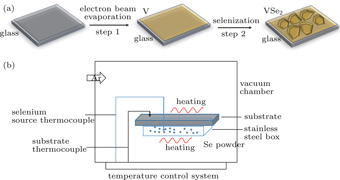
Fig. 1. (a) Schematic diagram of the synthesization of the VSe2 film with two-step method, (b) schematic diagram of the vacuum chamber for selenization process.

The specific selenization process is shown in Fig. 2(a). The substrate and the selenium source were simultaneously raised from room temperature to the same selenization temperature of 550 °C, which took 10 min. After 30 min of constant temperature, the selenium source started to cool down naturally. To prevent the substrate temperature from falling too fast and the condensed Se being absorbed onto the surface of the sample, we let the substrate be kept at a constant temperature for 15 min more than the selenium source and we also performed a degassing process when the substrate temperature was lowered from 550 °C to 300 °C.
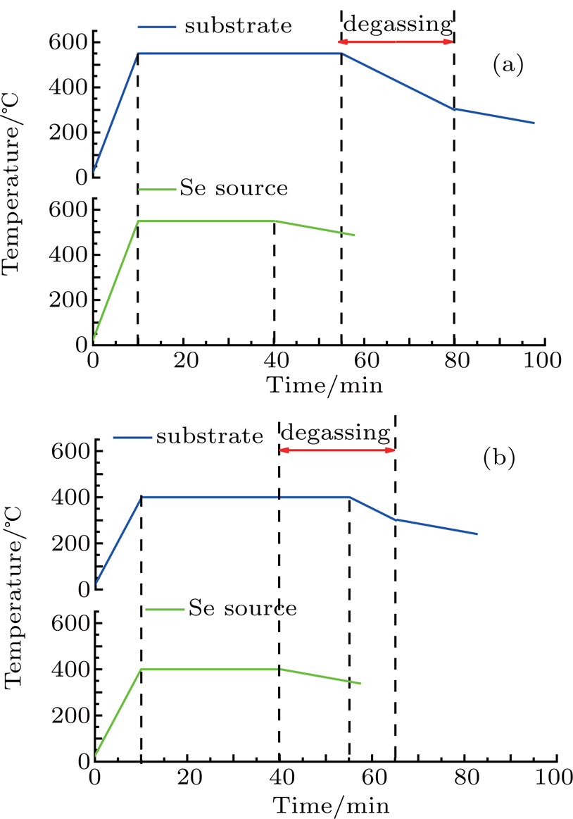
Fig. 2. (a) Selenization process at a selenization temperature of 550 °C and (b) at a temperature of 400 °C.

The phase structures of the films were measured by the PANalytical X’Pert pro x-ray diffractometer (XRD), which used Cu- (0.15418 nm) as the radiation source. The surface and profile of the films were observed by a Hitachi S-4800 field emission scanning electron microscope (SEM). The thickness of the films was measured by Ambios XP-2 model profiler. The current–voltage (JV) curve was measured by a solar simulator under the standard AM1.5 spectrum with illumination intensity of at room temperature. The optical properties of the films were observed by Varian’s Cary 5000 model UV–Vis–NIR spectrophotometer. The electrical properties of the films were measured by the Accent Optics Technology HL5550 Model Hall effect test system. X-ray photoelectron spectroscopy (XPS, Thermo Fisher ESCALAB 250 Xi) was used to detect the sample components. The excitation source used a monochromatic Al target (1486.6 eV) with an x-ray spot size of .

3. Result and discussion
3.1. Preparation of VSe2 thin film

Figure 3 shows the XRD pattern of the sample with 50 nm thick V film prepared on glass substrate at a selenization temperature of 550 °C. We can easily find the Se diffraction peak, which indicates that Se vapor is easily condensed. Thus, the surface of the sample is rich in selenium. However, no VSe2 peak is observed. A diffraction peak positioned at belonging to V3Se4 is observed. It is obvious that the crystallinity of V3Se4 is not very good. Unfortunately, we also obtain VO2. The appearance of oxide maybe because the oxygen in the air adhered to the surface of the V film before it was brought into the selenization chamber.

Fig. 3. XRD pattern of the sample with 50 nm thick V film selenized at 550 °C.

This experiment indicates that the selenization temperature is high. Then the selenization temperature was decreased to 400 °C. To prevent the appearance of Se on the surface of the film, the chamber is degassed as soon as the Se cools down, as shown in Fig. 2(b). Figure 4(a) shows the XRD pattern of a sample with 50 nm thick V film selenized at 400 °C. All the diffraction peaks can be indexed to the hexagonal VSe2 phase (JCPDS card #01-089-1641) without any other phases. This result is consistent with other reports.[10,19,21] In order to verify the stability of the selenization process, we selenized a 100 nm thick V film deposited on the glass with the same selenization process. Figure 4(b) shows the XRD pattern. The crystal structure of the formed VSe2 is confirmed to be a hexagonal phase without any impurity. The synthesized VSe2 film highly (00l) prefers this orientation. In particular, the intensity of each diffraction peak is much stronger than that of the VSe2 film prepared by selenizing the 50 nm V film. That is, the crystallinity of VSe2 is well improved, and the VSe2 preferential growth is along the c-axis. Figure 4(c) and 4(d) show the corresponding topographic images. Obviously, the sample obtained by selenizing a 50 nm thick V film is covered by some small nanosheets (Fig. 4(c)). The surface of the sample obtained by selenization of a 100 nm thick V film is covered with hexagonal nanosheets (Fig. 4(d)). These nanosheets on the surface of the sample grow very dense and have no holes or voids.

Fig. 4. XRD patterns and SEM images of the samples with (a), (c) 50 nm and (b), (d) 100 nm thick vanadium film selenized at 400 °C.

According to these results, VSe2 can be prepared by selenizing 50 nm-thick V film at 400 °C. Then 50 nm thick V films were selenized at different temperatures to study the VSe2 film growth behavior. Figure 5 shows the XRD patterns and the topographic SEM images of the corresponding films. At 350 °C, the XRD pattern exhibits a main diffraction peak (001) of VSe2, which grows along with the c-axis direction. At such growth temperature, the film is composed of some light white particles and layered sheets. As the temperature increases to 400 °C, the film is still (001) preferred orientation. However, the intensity of the Bragg peak (001) is significantly enhanced (as shown in Fig. 5(b)), which means that the crystal quality of VSe2 is improved. The inset SEM image indicates that the film consists of large and well-crystallized nanosheets, which is consistent with the corresponding XRD result. As the temperature increases further, the intensity of the (001) peak decreases and the peaks of V2O3 are detected, as shown in Figs. 5(c) and 5(d). Specially, VSe2 peaks cannot be detected and the film is composed of V2O3 entirely as the temperature increases to 500 °C. At such temperature, the films will not be composed of nanosheets, but small grains, as shown in the insets of Figs. 5(c) and 5(d). The oxidation of V should be the reason for the easier reaction between V and O2 at such high temperature than that between V and Se vapor, where O2 is possibility involved during transferring the formed V film from the growth chamber to the selenization chamber in atmosphere. These results indicate that the appropriate temperature for preparing the VSe2 layer on the glass should be about 400 °C.

Fig. 5. XRD patterns of the V films selenized at (a) 350 °C, (b) 400 °C, (c) 450 °C, and (d) 500 °C, the inset shows the corresponding SEM images of the films.

X-ray photoelectron spectroscopy (XPS) is carried out to further investigate the composition of the sample. The binding energies of 517.0 eV and 524.0 eV correspond to V 2p1/2 and 2p3/2, which indicate the V4+ state, as show in Fig. 6(a). The result is consistent with that in the references.[5,17,27] Figure 6(b) shows the XPS spectra of the Se 3d peak, the Se 3d5/2 (at 54.8 eV) and Se 3d3/2 (at 55.6 eV) peaks can be assigned to Se2−,[10,17,27,28] In addition, the binding energies (59.1 eV and 58.3 eV) of Se 3d match to those in SeO2.[28] The appearance of SeO2 can be considered as having some dangling bonds on the surface of the sample, and Se is combined with oxygen in the air to form a SeO2 phase. The depth of the sample detected by the XPS test is only a few nanometers, so the SeO2 phase can be clearly detected. We can conclude that the main component of the sample selenized at 400 °C is indeed VSe2.

Fig. 6. XPS spectra of (a) V 2p and (b) Se 3d regions for the sample of the 50 nm thickness V films selenized at 400 °C.

Optical properties of the as-grown thin films selenized at different temperatures are shown in Fig. 7. The sample of V thin film selenized at 400 °C has the highest reflectivity and the lowest transmittance. This indicates that VSe2 formed by the two-step process can be used in optoelectronic devices, especially in photovoltaic devices. VSe2 has the higher reflectivity and low transmittance. Because a VSe2 thin film is deposited between the back contact and the absorber layer, it can promote the re-absorption of sunlight and reduce the loss of light, which will promote the collection of photo-generated carriers.

Fig. 7. (a) Reflection and (b) transmission spectra of V thin films annealed at different temperatures.
3.2. Electrical properties of VSe2

If VSe2 is used in a solar cell, such as the kesterite structured solar cell, then it will be grown on Mo back contact film. Considering that the excessive thickness of the VSe2 layer deteriorates the performance of the device, we chose a 50 nm thick V film for research instead of 100 nm. Thus, we prepared a 50 nm thick V film on a Mo substrate. Both Mo and V films are preferentially grown in the (110) direction (Fig. 8(a)), the difference in the surface morphologies is not very obvious, as shown in Figs. 8(b) and 8(c). Both surfaces are covered with dense worm-like grains, but the grain size of the film covered with V is more uniform than that of Mo surface and the number of pores between grains is reduced. From the cross-sectional view in Fig. 8(d), we can see that the bond between V film and Mo substrate is very good, and no holes and gaps are formed at the Mo/V interface.

Fig. 8. (a) XRD patterns of Mo and V standard diffraction peaks, (b) SEM image of the Mo film, (c) vanadium film prepared on Mo substrate, (d) cross-sectional view of the vanadium film prepared on Mo substrate.

The V film prepared on Mo substrate was then selenized at the temperature of 400 °C. Figure 99(a) shows the XRD pattern of the sample. Due to the strong Mo diffraction peak, the diffraction peaks of others are too weak. In order to analyze the other phase, we cut off the Mo diffraction peak positioned at about –42°. It is obvious that the (001) and (002) crystal phases of VSe2 can also be obtained on the Mo substrate. At the same time, it also generates MoSe2. This happens because Se diffuses so fast that the VSe2 layer does not block the Se contacting with Mo to form MoSe2. The detailed morphologies and microstructures of the as-synthesized VSe2 nanosheets were investigated using SEM, as shown in Fig. 9(b). The surface of the sample is covered with a number of hexagonal nanosheets. It is also consistent with the morphology of the VSe2 prepared on the glass substrate. It shows that the stability of our two-step preparation of VSe2 process is very good.

Fig. 9. (a) XRD pattern and (b) SEM image of the VSe2 prepared on Mo substrate.

To understand the contact properties between Mo (metal) substrate and VSe2 (semiconductor material), we prepared a certain thickness of Al electrode on the Mo surface and VSe2 surface, and then performed the dark state IV test. In Fig. 10, the black curve represents the contact between Al/Mo, and the red represents the contact between Al/VSe2/Mo. It can be seen that the IV curve of the Al/Mo substrate is linear, which is a typical IV characteristic curve of ohmic contact. That is to say, the contact characteristic between Al and Mo is ohmic. The IV curve of the sample with the VSe2 film is also a linear straight line, so it can be concluded that there is ohmic contact between Al and VSe2 and Mo. This result shows that VSe2 can be well applied to semiconductor devices because of its good ohmic contact.

Fig. 10. Metal–semiconductor contact IV curve between Mo/Al and Al/VSe2/Mo.

In addition, we also performed a Hall test on the above samples. The test results are summarized in Table 1. The sample with VSe2 (0.2102 Ω/sq) has a lower square resistance than the molybdenum substrate without VSe2 (0.2135 Ω/sq). However, compared to the Mo substrate, the mobility of electrons is reduced. Because the carrier concentration of the VSe2 sample can reach the order of 1018. VSe2 can be well applied in semiconductor devices.

Table 1.

The Hall measurements of Mo substrate and VSe2 films prepared on Mo substrate.

.
4. Conclusion and perspectives

In summary, we demonstrate a new two-step route to synthesize the VSe2 film. By comparing the different selenization temperatures, we find that the VSe2 film has the best crystal quality when the selenization temperature is 400 °C. At 400 °C selenization temperature, we can stably prepare VSe2 film on both glass and Mo substrates. The XRD patterns of the VSe2 film indicate the VSe2 preferential growth along the c-axis. A number of hexagonal nanosheets can be clearly seen from the SEM image. Moreover, the sample of V thin film selenized at 400 °C has the highest reflectivity and the lowest transmittance. This indicates that VSe2 is well suited for application in optoelectronic devices. In addition, the contact between Al/VSe2/Mo belongs to ohmic contact, and the lower square resistance of VSe2/Mo sample can be observed. VSe2 is a potential material for solar cells. Moreover, this work opens up the opportunity for extensive research on the application of VSe2 in photovoltaic device or other semiconductor material devices.

Reference
[1] Manzeli S Ovchinnikov D Pasquier D Yazyev O Kis A 2017 Nat. Rev. Mater. 2 17033
[2] Tan C Lai Z Zhang H 2017 Adv. Mater. 29 1701392
[3] Lin X Wang J 2017 Acta Chim. Sin. 75 979
[4] Novoselov K S Mishchenko A Carvalho A Castro Neto A H 2016 Science 353 9439
[5] Zhao W Dong B Guo Z L Su G Gao R J Wang W Cao L X 2016 Chem. Commun. (Camb) 52 9228
[6] Xu K Chen P Z Li X L Wu C Z Guo Y Q Zhao J Y Wu X J Xie Y 2013 Angew Chem. Int. Ed. Eng. 52 10477
[7] Marri S R Ratha S Rout C S Beheraet J N 2017 Chem. Commun. (Camb) 53 228
[8] Vatansever E Sarikurt S Evans R F L 2018 Mater. Res. Express. 5 046108
[9] Bonilla M Kolekar S Ma Y Diaz H C Kalappattil V Das R Eggers T Gutierrez H R Phan M H Batzillet Ma 2018 Nat. Nanotechnol 13 289
[10] Zhang Z P Niu J J Yang P F Gong Y Ji Q Q Shi J P Fang Q Y Jiang S L Li H Zhou X B Gu L Wu X S Zhang Y F 2017 Adv. Mater. 29 1702359
[11] Hayashi K Nakahira M 1978 J. Soild State Chem. 24 153
[12] Whittingham M S 1978 Mat. Res. Bull. 13 959
[13] Nikonov K S Brekhovskikh M N Egorysheva A V Menshchikova T K Fedorovet V A 2017 Inorg. Mater. 53 1126
[14] Yang J Y Wang W K Liu Y Du H F Ning W Zheng G L Jin C Han Y Y Wang N Yang Z R Tian M L Zhang Y H 2014 Appl. Phys. Lett. 105 063109
[15] Claessen R Schafert I Skibowski M 1990 J. Phys.: Condens. Matter 2 10045
[16] Hossain M Wu J X Wen W Liu H N Wang X S Xie L M 2018 Adv. Mater. Interfaces 5 1800528
[17] Wang C L Wu X Ma Y H Mu G Li Y Y Luo C Xu H J Zhang Y Y Yang J Tang X D Zhang J Bao W Z Duan C G 2018 J. Mater. Chem. 6 8299
[18] Hector A L Jura K Levason W Reid S D Reidet G 2009 New J. Chem. 33 641
[19] Zhang Z P Gong Y Zou X L Liu P Yang P F Shi J P Zhao L Y Zhang Q Gu L Zhang Y F 2018 ACS Nano 10.1021/acsnano.8b08677
[20] Lee S Kim J Park Y C Chun S H 2019 Nanoscale 11 431
[21] Ming F W Liang H F Lei Y J Zhang W L Alshareef H N 2018 Nano. Energy 53 11
[22] Lin H He S J Mao Z Miao J Xu M Li Q 2017 Nanotechnology 28 445603
[23] Wang Y P Qian B B Li H H Liu L Chen L Jiang H B 2015 Mater. Lett. 141 35
[24] Wang D L Bai Z Z Yang R L Hou Z R 2013 Physics 42 346
[25] Gao S S Jiang Z W Wu L Ao J P Zeng Y Sun Y Zhang Y 2018 Chin. Phys. 27 018803
[26] Liu Z L Wu X Shao Y Qi J Cao Y Huang L Liu C Wang J O Zheng Q Zhu Z L Ibrahim K Wang Y L Gao H J 2018 Sci. Bull. 63 419
[27] Ulusoy Ghobadi T Patil B Karadas F Okyay A K Yilmaz E 2017 ACS Omega. 2 8319
[28] Cao Q Frank F Y Lina S Xiang F X Liu G L Wang X L 2017 Nanotechnology 28 475703