Two-step growth of VSe2 films and their photoelectric properties
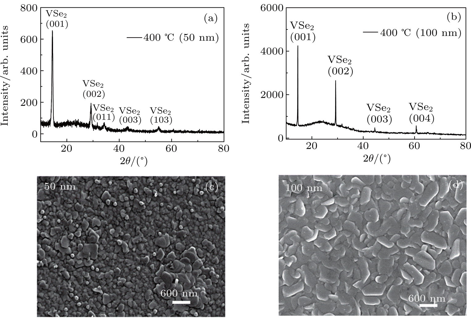
XRD patterns and SEM images of the samples with (a), (c) 50 nm and (b), (d) 100 nm thick vanadium film selenized at 400 °C.

Two-step growth of VSe2 films and their photoelectric properties |
|
XRD patterns and SEM images of the samples with (a), (c) 50 nm and (b), (d) 100 nm thick vanadium film selenized at 400 °C. |
 |