Project supported by the Advanced Research Foundation of China (Grant No. 914xxx803-051xxx111), the National Defense Advanced Research Project of China (Grant No. 315xxxxx301), and the National Defense Innovation Program of China (Grant No. 48xx4).
Project supported by the Advanced Research Foundation of China (Grant No. 914xxx803-051xxx111), the National Defense Advanced Research Project of China (Grant No. 315xxxxx301), and the National Defense Innovation Program of China (Grant No. 48xx4).
† Corresponding author. E-mail:
Project supported by the Advanced Research Foundation of China (Grant No. 914xxx803-051xxx111), the National Defense Advanced Research Project of China (Grant No. 315xxxxx301), and the National Defense Innovation Program of China (Grant No. 48xx4).
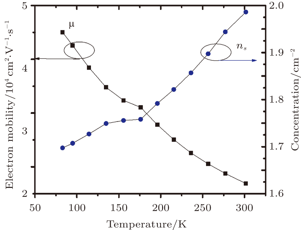
In this report, the effect of temperature on the InAs/AlSb heterojunction and high-electron-mobility transistors (HEMTs) with a gate length of 2 μm are discussed comprehensively. The results indicate that device performance is greatly improved at cryogenic temperatures. It is also observed that the device performance at 90 K is significantly improved with 27% lower gate leakage current, 12% higher maximum drain current, and 22.5% higher peak transconductance compared to 300 K. The temperature dependence of mobility and the two-dimensional electron gas concentration in the InAs/AlSb heterojunction for the temperature range 90 K–300 K is also investigated. The electron mobility at 90 K (42560 cm2/V·s) is 2.5 times higher than its value at 300 K (16911 cm2/V·s) because of the weaker lattice vibration and the impurity ionization at cryogenic temperatures, which corresponds to a reduced scattering rate and higher mobility. We also noted that the two-dimensional electron gas concentration decreases slightly from 1.99 × 1012 cm−2 at 300 K to 1.7 × 1012 cm−2 at 90 K with a decrease in temperature due to the lower ionization at cryogenic temperature and the nearly constant ΔEc.
In recent years, InAs/AlSb HEMTs have become one of the most promising candidates for high-speed, low-power, and low-noise applications.[1,2] A very important application of these transistors is for low noise amplifiers (LNA) that are used in deep space exploration, and are operated primarily at cryogenic temperatures to improve the sensitivity of detection.
During the past twenty years, InP HEMTs have been the dominant force in microwave millimeter wave applications.[3,4] Compared with InP HEMTs, InAs has a higher electron mobility and saturation drift speed. Moreover, InAs/AlSb HEMTs exhibit a two-dimensional electron gas (2-DEG) distribution in the channel due to the small lattice mismatch between the InAs and AlSb and the large conduction band offset (about 1.35 eV) that can form deep quantum wells. Therefore, the application of InP HEMTs for use in cryogenic LNAs has recently been challenged by InAs/AlSb HEMTs. In Ref. [5], the first demonstration of an InAs/AlSb HEMT LNA at cryogenic temperatures was reported. At room temperature, the three-stage amplifier exhibited a transducer gain of 29 dB and a noise temperature of 150 K with 17.6 mW power consumption. At cryogenic temperatures, the optimum drain voltage for best noise performance was reduced from 0.55 V to 0.3 V, demonstrating the very low-power and low-voltage capabilities of InAs/AlSb HEMTs-based low-noise amplifiers. InAs/AlSb HEMTs are typical 2DEG-based devices with electrical characteristics that are very sensitive to the operating temperature. The cryogenic characteristics of InAs/AlSb HEMTs are determined by the temperature dependency of the electron mobility and 2-DEG in the InAs channel. The characterization of electron mobility and 2-DEG at different temperatures will assist in improving the general understanding of the change mechanism of the drain current, gate-leakage currents and transconductance.
In this work, the temperature effect on InAs/AlSb heterojunction and HEMTs are comprehensively discussed. The results indicate that device performance is greatly improved at low temperatures. It has also been observed that the leakage current decreases with a reduction of the to 90 K because of the Schottky leakage current component and the hole leakage current component caused by the impact ionization effect decreased. The decrease of the gate–leakage currents with temperature is a clear advantage for devices operating at cryogenic temperatures. The temperature dependence of the mobility and the two-dimensional electron gas concentration in InAs/AlSb heterojunctions in the temperature range 90 K–300 K is also investigated. The lower lattice vibration and the impurity ionization at cryogenic temperatures correspond to a reduced scattering rate and higher mobility. The two-dimensional electron gas concentration decreases slightly with the decrease of temperature due to the lower ionization at cryogenic and the nearly constant ΔEc.
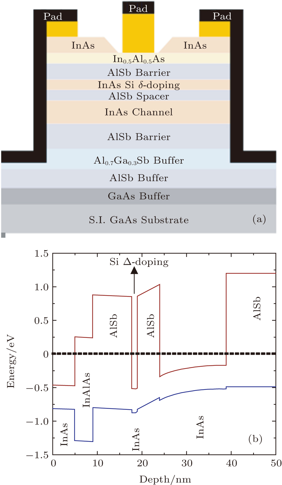
Before device fabrication, the material is grown by molecular beam epitaxy (MBE). The material structure and its energy band diagram are illustrated in Figs.
An alloyed Ohmic contact is formed by e-beam evaporation of Pd/Ti/Pt/Au (20/30/30/30 nm), following by RTA at 300 °C for 20 s. The contact resistance Rc and contact resistivity ρc are 0.116 Ω·mm and 3.50 × 10⁻⁷ Ω·cm2, respectively, for TLM at 300 K. Optical images of TLM pattern, I–V curves of two contacts with different dn, and Rtot as a function of dn are shown in Figs.
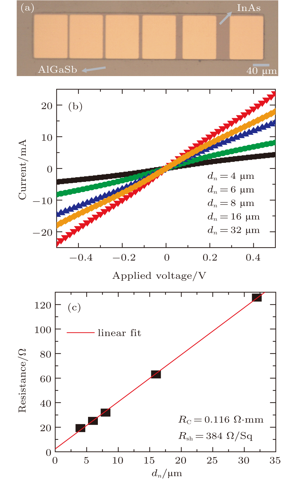 | Fig. 3. (color online) (a) Optical image of TLM pattern, (b) I–V curves of two contacts with different dn at 300 K, and (c) Rtot as a function of dn. |
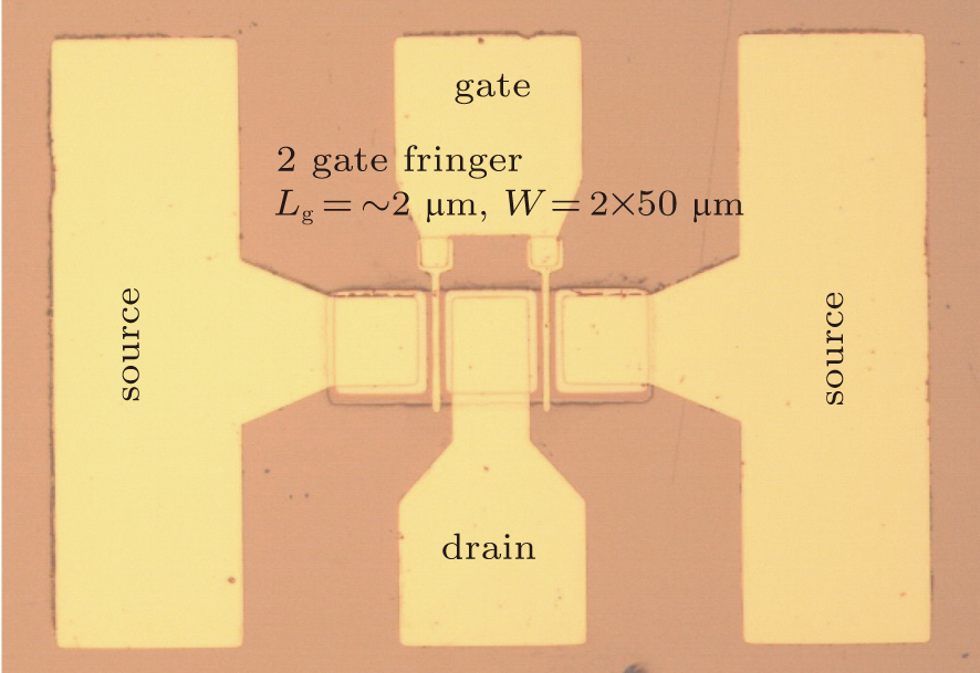
Before Schottky gate metal deposition, gate recess etching is performed using a citric acid/H2O2 solution in order to avoid gate-to-source and gate-to-drain conduction, because of the highly doped InAs cap layer. Then, the Schottky gate metal is deposited by e-beam evaporation of Ti/Pt/Au (20/20/300 nm). Finally, a probing pad is deposited by e-beam evaporation of Ti/Au (20/300 nm). A gate width of 50 μm and a gate length of 2 μm are used, as shown in Fig.
The cryogenic characteristics of InAs/AlSb heterojunctions are determined by the cryogenic characteristics of a 2-DEG in an InAs channel, in which the temperature dependency of mobility and the density of electrons is important.
The electron mobility μ refers to the average speed of electrons units under the influence of the electric field, which is determined by scattering mechanism. The value of μ can be obtained from the relaxation time τ, which is inversely proportional to the scattering probability P;
 |
There are three primary scatter mechanisms for mobility in the InAs channel: ionized impurity scattering, lattice vibration scattering, and interface roughness scattering.[6–8]
 |
As the temperature decreases, the lattice vibration and the impurity ionization decrease, which results in reduced scattering rate and higher mobility. The interface roughness scattering is associated with the two-electron gas density.
Figure
The 2-DEG is generated in the InAs channel on the side of the InAs/AlSb heterostructure It can be seen from Fig.
(i) From 300 K to 175 K, the concentration ns decreased rapidly because the ionization rate of impurities decreased significantly. Below 175 K, the concentration decreased slowly because the ionization rate of impurities cannot be significantly reduced any further.
(ii) The relationship between the InAs bandgap and temperature can be expressed by
 |
 |
The conduction band offset ΔEc[9] at different temperatures are shown in Table
| Table 1. ΔEc at different temperatures. . |
It can be seen from the previous analysis that the 2-DEG concentration decreases slightly with a decrease in temperature because of the diminished ionization at cryogenic temperatures.
Electrical measurements are performed using a cryogenic probe station Lakeshore CRX-4K to connect an Agilent B1500A at room temperature (300 K) and at a cryogenic temperature (90 K). When the temperature is reduced to 90 K, the device performance is greatly improved.
Figure
 |
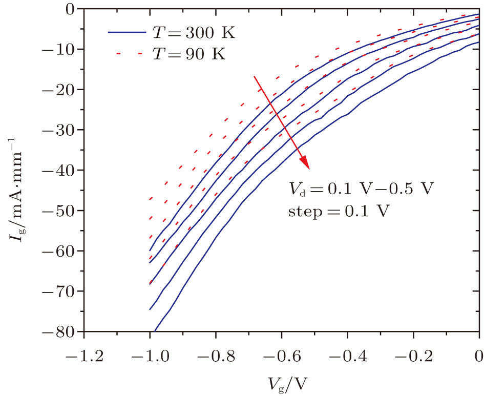 | Fig. 6. (color online) Ig (Vg) with Vd ranging from 0.1 V to 0.5 V in steps of 0.1 V at 300 K (solid lines) and 90 K (dot lines). |
i) The Schottky leakage current as a function of temperature is given by
 |
 |
 |
ii) The impact ionization effect means that the collision between carriers and lattice atoms will generate redundant electron–hole pairs because the carriers in the channel experience an increase in energy as the applied voltage is increased. Thus, it can be seen from Fig.
Figure
 | Fig. 7. (color online) Id (Vd) with Vg ranging from −1 V to 0 V in steps of 0.1 V at 300 K (solid lines) and 90 K (dot lines). |
In the linear region, the drain current is given by
 |
 |
It can be seen from Fig.
Figure
 | Fig. 8. (color online) (a) gm (Vg) at 300 K and 90 K for drain voltages of 0.1 to 0.5 V. (b) Peak gm (Vd) at 300 K and 90 K. |
The relationship between the transconductance and the drain voltages can be expressed by
 |
We report on studies on the room temperature and cryogenic performance of InAs/AlSb high-electron-mobility transistors (HEMTs) with a gate length of 2 μm, which exhibits significant improvement in device performance at low temperatures. It has been observed that the leakage current decreases when the temperature is reduced to 90 K. This is because of the Schottky leakage current component and the hole leakage current component caused by a decrease of the impact ionization effect. The temperature dependence of the mobility and the two-dimensional electron gas concentration in InAs/AlSb heterojunctions in the temperature range 90 K–300 K is also investigated. The weaken lattice vibration and the impurity ionization at cryogenic temperatures correspond to a reduced scattering rate and higher mobility. The two-dimensional electron gas concentration decreased slightly with a decrease in temperature due to the weakened ionization at cryogenic temperatures and the nearly constant ΔEc. Overall, it is observed that the performance of InAs/AlSb HEMTs is greatly improved at cryogenic temperatures, which is more amenable to the applications of ultra-high speed and low dissipation circuits.
| [1] | |
| [2] | |
| [3] | |
| [4] | |
| [5] | |
| [6] | |
| [7] | |
| [8] | |
| [9] | |
| [10] | |
| [11] |


