Etching-assisted femtosecond laser microfabrication*

Project supported by the National Natural Science Foundation of China (Grant No. 51501070).

Liu Monan1, Li Mu-Tian2, Yang Han2, †, Sun Hong-Bo2
Department of Condensed Matter, College of Physics, Jilin University, Changchun 130012, China
State Key Laboratory on Integrated Optoelectronics, College of Electronic Science and Engineering, Jilin University, Changchun 130012, China


† Corresponding author. E-mail: yanghan@jlu.edu.cn

Project supported by the National Natural Science Foundation of China (Grant No. 51501070).

Abstract

Although femtosecond laser microfabrication is one of the most promising three-dimensional (3D) fabrication techniques, it could suffer from low fabrication efficiency for structures with high 3D complexities. By using etching as a main assistant technique, the processing can be speeded up and an improved structure surface quality can be provided. However, the assistance of a single technique cannot satisfy the increasing demands of fabrication and integration of highly functional 3D microstructures. Therefore, a multi-technique-based 3D microfabrication method is required. In this paper, we briefly review the recent development on etching-assisted femtosecond laser microfabrication (EAFLM). Various processing approaches have been proposed to further strengthen the flexibilities of the EAFLM. With the use of the multi-technique-based microfabrication method, 3D microstructure arrays can be rapidly defined on planar or curved surfaces with high structure qualities.

1. Introduction

With the increase of the demands in the manufacturing of various micro–nano devices, femtosecond laser direct-writing (FsLDW) has attracted significant interest owing to its ability for high-performance three-dimensional (3D) fabrication.[114] The non-linear nature of the FsLDW can satisfy the stringent requirements in terms of both high fabrication precision and flexible designability, making it well applicable in optics,[1517] photochemistry,[18] optoelectronics,[19] nanophotonics,[20] etc. The ultra-high energy of the femtosecond laser pulse enables fine processing of materials through two-photon polymerization or laser ablation.[1] Various materials can be processed by FsLDW, from soft materials[2123] to various hard substrates.[24,25] The point to point processing of this technique can realize various 3D structure designs, such as meta-surfaces[20] and waveguides.[17] As a complementary fabrication technique of photolithography, FsLDW is mostly targeted on functional complex 3D structures, which exceed the processing ability of photolithography. Many of these functional structures contain hierarchies or arrays, which are very common in biomimetic and optoelectronic devices. In particular, FsLDW is expected to realize complex 3D structures on curved surfaces by point to point scanning throughout the volume.[1] Although the powerful 3D femtosecond laser microfabrication (3D FsLMF) can achieve the above structuring, it is time-consuming for complex 3D micro-nanostructures.

We consider the structure of microlens arrays as an example. Inspired by the structure of insect compound eyes, the microlens arrays possess the extraordinary optical properties of their natural counterparts, such as a large field of view (FOV) and multi-aperture.[26] As an assembly of thousands of ommatidia, the microlens arrays can be regarded as a typical 3D configuration set on a curved surface. In this case, FsLDW is considered the most suitable technique to realize such complex 3D microstructures. However, considering the large number of ommatidia, the fabrication of such structures can last hours owing to the point to point scanning of FsLDW.[26] In order to increase the fabrication efficiency, a series of conventional machining methods assisted by FsLDW have been developed.[24,2729] For example, chemical etching has already been introduced as an assistant technique, which can effectively improve the efficiency of FsLMF.[24,28] The etching-assisted femtosecond laser microfabrication (EAFLM) can be considered a two-step fabrication process, consisting of laser seeding and etching based on the seeds. In the first step, femtosecond laser ablation forms a pattern of microhole arrays on the substrate by point to point scanning. The high-energy laser pulse significantly modifies these local regions and generates seeds by permanently changing their chemical properties.[30] In the second step, acids or alkali solutions help perform a fast etching of the seed regions. The etching finally shapes the microholes into desired structure profiles and smoothens the structure surface.[24] Although wet etching can help accelerate the fabrication of complex 3D microstructures, it could lead to structure distortion and incompatibility in post device integrations.[30] The fabrication efficiency can be decreased for 3D microfabrications on curved surfaces, e.g., fabrication of compound eyes. This occurs as the scanning over curved surfaces relies on a complex time-consuming 3D stage manipulation of the femtosecond laser focus. In addition, the present EALMF has been limited to a few materials owing to the material selectivity of chemical etching.[28,29] These issues are beyond the capability of any single technique; therefore, a multi-technique solution is needed.

Extensive studies have been performed to overcome the above technical obstacles in 3D FsLMF. With the assistance of etching (either dry or wet), both fabrication efficiency and structure surface quality can be significantly improved. A flexible combination of EAFLM and conventional rapid prototyping methods can realize fast fabrications of complex 3D microstructures on curved surfaces. Targeting on the 3D structures of artificial compound eyes and their analogs (microlens arrays), we systematically introduce the newly developed EAFLM methods, including their fabrication schemes, main setups, key-parameter controls, and preliminary results.

2. Experimental setup

In this section, the main experimental setups of EAFLM are introduced, including a typical 3D FsLMF system, a single-pulse laser seeding system, and a dry-etching system used in the above studies.

2.1. 3D FsLMF system

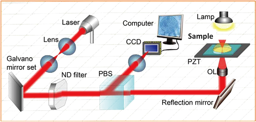
Figure 1 shows a schematic of a typical 3D FsLMF system, which can be divided into four subsystems according to their distinct functions: a femtosecond laser source with a beam-directing system (left column), a beam-rotating and -travelling stage (right column), and an instantaneous monitoring system (middle column). The fourth subsystem is a digital-image-generation subsystem, which is not included in the schematic. Under the control by the computer of the monitoring subsystem, the femtosecond-laser beam focus irradiates the sample on the motion stage and modifies local regions with its high energy pulse. These femtosecond-laser-modified local regions are chemically distinct from the unmodified regions, leading to an etching rate difference in the following etching process. The most commonly used laser source for 3D FsLMF is a Ti:sapphire femtosecond laser system, with a central wavelength of 800 nm, pulse duration of 100 fs, and repetition rate of 1 kHz.[1]

Fig. 1. (color online) Schematic of the 3D FsLMF system. The core components of the system are the femtosecond laser system and tightly focused high-numerical-aperture-(NA) lens (1.4, oil immersion). Two key controlling factors of the high fabrication precision are the stability of the pulse laser energy output and the scanning accuracy of the focus/sample. A charge-coupled-device (CCD) camera is used as the imaging system for optical modulation and monitoring. In the setup shown in the figure, other optical components are also included such as the polarization beam splitter (PBS), objective lens (OL), and piezoelectric transducer (PZT).[1]
2.2. Single-pulse laser-seeding system

The single-pulse laser-seeding system uses a spatial light modulator (SLM) to modulate the wavefront of the femtosecond laser beam in the 3D FsLMF system. The modulated wavefront forms a designable wavelet pattern for a multi-wavelet irradiation on the substrate. Such modulation enables a pattern of laser seeds by one single pulse instead of a point by point seeding, which increases the laser-seeding efficiency a lot. The system setup is shown in Fig. 2(a). The frequency-doubled femtosecond laser beam was led through a telescope for a triple expansion by two lenses with focal lengths of −50 mm and 150 mm. The laser beam was then directed onto a reflection phase-only liquid-crystal-on-silicon SLM (LCOS-SLM, LETO, HOLOEYE Photonics AG) for phase modulation. The modulation provided 256 phase levels and full high definition (FHD) over a 1920 × 1080 pixel area. Its pixel pitch was set to be 6.4 μm with an inter-pixel gap of 0.2 μm, ensuring a high fill factor (93%) and output efficiency. The maximum accommodated power density was ∼ 2 W/cm2. The modulation was performed according to a pre-imported computer-generated hologram (CGH, resolution 1024 × 1024) using the optimal rotation-angle (ORA) method. After modulation, the pattern of multi-beams was directed to the entrance of a planar objective (NA = 0.7) by a 4-f optical system, including two plano-convex lenses (focal lengths: 400 mm and 300 mm). The output multi-beams were focused on the substrate surface, where the multi-beam exposure led to a corresponding pattern of multiple laser seeds. The substrate was supported by a motorized xy stage powered by a step motor (resolution: 100 nm, maximum stroke: 20 mm). The focusing was controlled by a piezo z stage (resolution: 1 nm, maximum stroke: 100 μm). In addition, the 0th-order light was isolated in the z direction or the xy plane to avoid unwanted influence.[31]
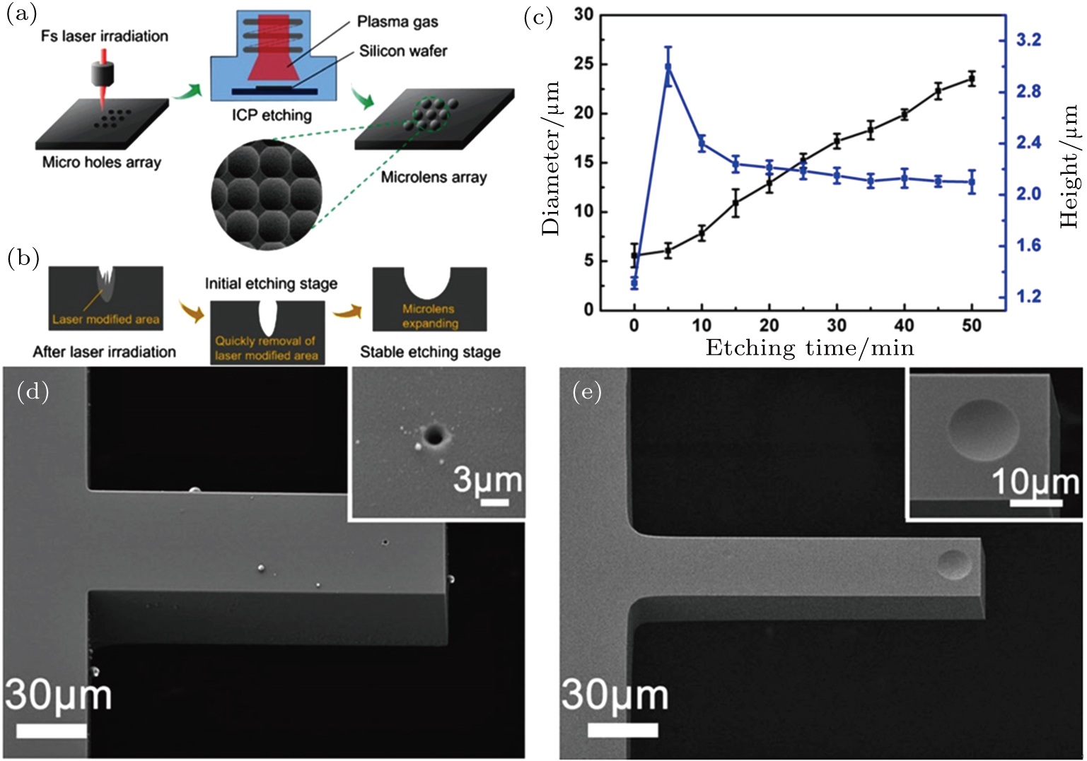
Fig. 2. (color online) Dry-etching-assisted 3D FsLMF. (a) Schematic of the fabrication process, including a point-by-point laser-seeding and dry-etching as two main steps. (b) Schematic of the profile evolution of a local laser-modified region during the dry etching. (c) Dependences of the diameter and height on the etching time. (d) and (e) High compatibility of the dry-etching-assisted 3D FsLMF: scanning-electron-microscopy (SEM) images of (d) a laser seed (microhole) and (e) concave microlens integrated on a microcantilever; magnified images are shown in the insets.[30]
2.3. Dry-etching system

The employed dry-etching system is an inductively-coupled-plasma (ICP, ULVAC CE 300I) instrument, illustrated in Fig. 2(a). The following etching parameters were used: APC pressure of 1 Pa, trigger pressure of 5 Pa, PFC pressure of 5 Pa, antenna radio-frequency (RF) power of 400 W, and bias RF power of 40 W. The etching time was determined according to the specific structures, varied from tens of minutes to hours.[30]

3. Results and discussions
3.1. Dry-etching assisted 3D FsLMF

As discussed above, the unique functions of bio-inspired structures depend closely on their complex and fine 3D structure arrangements.[26] Therefore, a high structure quality needs to be ensured when EAFLM is used to fabricate these microstructures, such as microlens arrays. As a typical material-removal process, the femtosecond laser ablation can lead to an intolerable surface roughness when operated with a high laser power. The fierce scattering of particles due to laser bombardment significantly roughens the structure surface, thus degrading the functionality. A possible solution is to reduce the laser power to suppress the laser-ablation-induced surface roughness. Dry-etching is proposed as an alternative assistant technique to fabricate microlens structures based on laser patterning. Compared with the chemical-etching-assisted FsLMF discussed in Section 1, the dry-etching-based processing method provides a significantly higher processing accuracy as well as higher compatibility for post-integration,[30] as in chemical etching, lateral etching can occur when the etched structures are integrated to a target substrate. This leads to incompatibility between the two components. Dry etching does not suffer from such incompatibility as the etching medium is plasma gas rather than acid.

The fabrication procedure is shown in Fig. 2(a). First, a relatively low laser power was chosen to perform the laser ablation. According to the desired microlens structures, a series of microhole arrays were patterned on a silica substrate by the femtosecond laser ablation. The microhole arrays were then set in the ICP chamber and etched. More information on the ICP instrument is provided in Subsection 2.3. This two-step fabrication strategy can be described as a seeding–etching process. In the seeding session, the femtosecond laser ablation seeds the material with microholes. In the etching session, the SF6 etching plasma helps shape each local seed into a concave profile. Figure 2(b) shows the schematic evolution of a local microhole profile. After the laser ablation, a microhole was formed, whose local region was significantly modified by the high-energy pulse of the femtosecond laser beam. The inside of the microhole was very rough after the laser ablation. As the etching progressed, the plasma etched both laser-modified and unmodified regions. The etching expanded the microhole profile while removing the scattered particles by the laser ablation. The dry etching was performed in an ICP instrument owing to its flexible etching control on each dimension. With the progress of the etching, the microholes gradually laterally expanded and finally evolved into the desired microlens structures.

Figure 2(c) shows the evolutions of the diameter and height of a single microhole during the dry-etching process. Unlike the behavior in wet etching, the different evolutions along the lateral and vertical directions indicate an anisotropic nature of the dry etching. The diameter increases with the etching time following an approximately linear tendency. This suggests that the lateral etching rate was almost stable throughout the etching process. The uniform lateral etching rate can be attributed to the synchronous etching of laser-modified and unmodified regions. The etching rates of the two regions can be estimated based on the cross-section characterization of a microhole etched for a varied time duration. We obtained values of 4 μm/s for the laser-modified region and 1 μm/s for the unmodified region. The laser modification significantly increases the etching rate as the laser ablation with an ultra-high pulse energy can significantly modify the local chemical properties of the processed material. We consider a Si substrate as an example. With the absorption of the laser pulse energy, local atoms excite and even reorganize. Consequently, the laser-modified regions become polycrystalline, which enables a significantly higher etching rate. For the evolution of the microhole depth, the behavior is apparently different. The depth of the microhole initially rapidly increases and then decreases. The decrease slows down after an etching duration of 15 min and finally approaches a steady value. The self-limitation of the etching depth is due to the aperture effect. This effect originates from the plasma gas exhaustion when the vertical etching proceeds to a certain depth. The local gas exhaustion could significantly decrease the vertical etching rate. The case of reaction product exhaustion correspondingly exhibits the same behavior. Therefore, after the early increase stage of the microhole depth (within 5 min), the vertical etching rate of the laser-modified regions decreases very rapidly owing to the aperture effect. In addition to the dependence on the etching time, the profile of the obtained microlenses is also dependent on the laser power and pulse number. With the increase of the laser power or pulse number, both the diameter and depth of the microlenses increase. The surface quality improvement of the dry etching after the laser ablation was also demonstrated by an atomic-force-microscopy (AFM) characterization. The surface roughness of a laser-ablated silicon wafer can be significantly decreased from 175 nm to 8 nm, very close to that of a dry-etched-only wafer (5.6 nm). Figures 2(c) and 2(d) demonstrate the high compatibility of the dry-etching-based EAFLM. The SEM images show that a laser seed could be directly defined on a microcantilever and then evolved into a concave microlens after etching. The microcantilever remained intact during the microlens integration. With the high compatibility of the dry-etching-assisted FsLMF, functional 3D microstructures can be well integrated to desired devices.[30]

3.2. Single-pulse-enabled laser seeding

The functional optical structures of microlens arrays can be well fabricated by EAFLM by means of either wet or dry etching. The fabrication strategy is described as a seeding–etching process. In the previous section, dry etching was used as an alternative assistant method to speed up the prototyping with higher precision and integration compatibility. However, the processing efficiency is still restricted by the point-to-point seeding step, i.e., the femtosecond laser beam needs to be well manipulated to pattern the seeds one by one along the substrate surface. The number of seeds can be large, from several hundreds to thousands, aiming at specific functional structures such as compound eyes. In this case, the 3D fabrication efficiency needs to be further increased by radically changing the laser seeding methodology. SLM is suitable for this scheme as it can modulate the laser wavefront into a pattern of energy-varied wavelets. The number and topology of these wavelets can be pre-arranged according to the specific array structure design. With the assistance of the SLM, a pattern of wavelets can be seeded into the substrate surface with a single-pulse shot. By combining this single-pulse seeding process with wet etching, the fabrication of microlens arrays can be accelerated without any compromise in the fabrication precision.[31]

Figure 3(a) shows the schematic setup of the single-pulse-seeding EAFLM system. The femtosecond laser beam was led onto a reflection phase-only liquid-crystal-on-silicon SLM before being expanded three times. The coordinates of the wavelets were pre-recorded together with their relative energies, forming a series of digital representatives. The specific location and energy of each wavelet were determined according to the individual microlens size and pattern of the desired arrays. These digital representatives were transformed to a wavelet hologram and then loaded on the controlling computer of the SLM for a desired wavefront modulation. With this approach, a multi-beam output was generated, directed through two plano-convex lenses, and finally focused on the substrate surface. More details about the SLM and setup have been provided in Subsection 2.2. An example of the multi-beam pattern, i.e., an array of seeds enabled by a single pulse, is illustrated in Fig. 3(b). Each circle size corresponds to its relative energy Ei (e.g., i = 1, 2, 3,…, 9 in Fig. 2(b)), as the exposure dose determines the size of the permanently laser modified regions. Figures 3(c) and 3(d) show an array of nine concave microlenses chemically etched from a 3 × 3 seed array (40 min in 20 vol.% HF), in both top and side views. The obtained microlenses are conformal and have a high surface smoothness, indicating a high fabrication quality provided by this single-pulse-seeding method. The sizes of these microlenses are independently and highly designable by initially setting the relative energy of each seed. Based on the accurate control of the seed array organization, size-varied hexagonally patterned microlens arrays can be well fabricated using the single-pulse-seeding method, as shown by the SEM image in Fig. 3(e). The seed energies of the microlenses were initially set to 1, 0.9, 0.8, and 0.7, from the array center to the edge, as shown by the inset. The original laser pulse energy irradiated to the SLM was 7.1 μJ, while the etching time was 40 min.[31] With further investigations, this highly efficient and designable laser-seeding method could provide novel functional structures in various application fields.
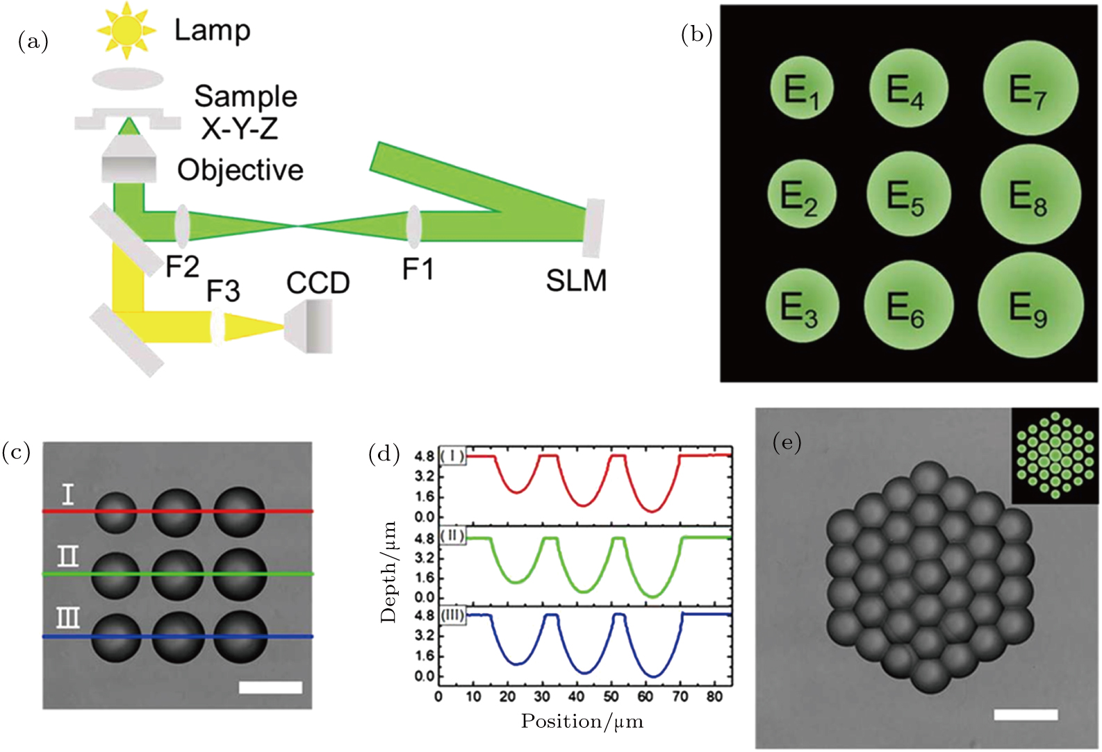
Fig. 3. (color online) 3D FsLMF through single-pulse-enabled laser seeding. (a) Schematic of the fabrication system with an SLM to realize single-pulse laser seeding. (b) Schematic of a 3 × 3 seed array obtained from modulated multi-beams with varied powers, where the circle size represents the corresponding power. (c) Confocal microscopic image and (d) AFM cross-section characterizations of a fabricated 3 × 3 concave microlens array. (e) Confocal microscopic image of a hexagonally arranged densely packed concave microlens array; the inset shows its schematic seed pattern.[31]
3.3. Wet-etching-assisted FsLMF on curved surfaces

Although the flexible EAFLM can realize microlens arrays with high precision and fill factor, there are still some challenges toward the realization of real artificial compound eyes. For example, most of the bio-inspired microstructures fabricated using the EAFLM are obtained by laser seeding and post-etching on planar substrates, while the natural compound eye structure consists of a large number of ommatidia on a curved macroscopic base. The laser writing on curved surfaces requires complex manipulation of the laser focus through a high-precision platform. The stringent setup requirement significantly limits the fabrication efficiency and throughput. In this case, methods such as structure transfer or post-substrate-bending have been proposed to help realize fast fabrications of large-scale (millimeter) microstructures on curved surfaces.[32,33] However, owing to the strain distribution on the curved surfaces, these methods tend to cause unavoidable structure deformations as well as device degradation. Novel strategies aiming at fast 3D microfabrications on curved surfaces or substrates are required.[26,34]

Thermal embossing is a feasible method for a fast fabrication of compound eye structures with soft materials. Figure 4(a) shows such a fabrication process using double thermal embossing. This process can be divided into three steps. First, a master mold was fabricated using wet-etching-based EAFLM. An array of concave microlenses was obtained on the planar mold substrate (silica glass). Second, the glass master mold was turned upside down and placed onto a prepared poly(methyl methacrylate) (PMMA) slice. The reverse structure of the master mold, i.e., an array of convex microlenses, was thermally embossed on the PMMA slice at 95 °C. Finally, the peeled-off planar convex microlens arrays underwent second thermal embossing with a pre-heated glass bead (100 °C) to acquire a macroscopic curvature. A PMMA compound eye structure with hundreds of ommatidia has been obtained by thermal structure transfer and deformation. Figure 4(b) shows the overall and local morphologies of the planar convex microlens arrays obtained by the first thermal embossing. A large number of densely packed concave microlenses could be formed by the first thermal embossing, suggesting high throughput and structure quality. The PMMA convex microlens arrays have an average diameter of 24.5 μm and average sag height of 4.67 μm. The diameter deformation ratio is estimated to be ∼1%, indicating that the thermal embossing ensures structure fidelity. After the second thermal embossing, the planar macroscopic profile of the convex microlens arrays was well transformed to a spherical profile, as shown in Fig. 4(c). The spherical surface is composed of hundreds of densely packed convex microlenses, with a higher fill factor, very close to 100%. The structure is very similar to those of natural compound eyes, both microscopically and macroscopically.[26]
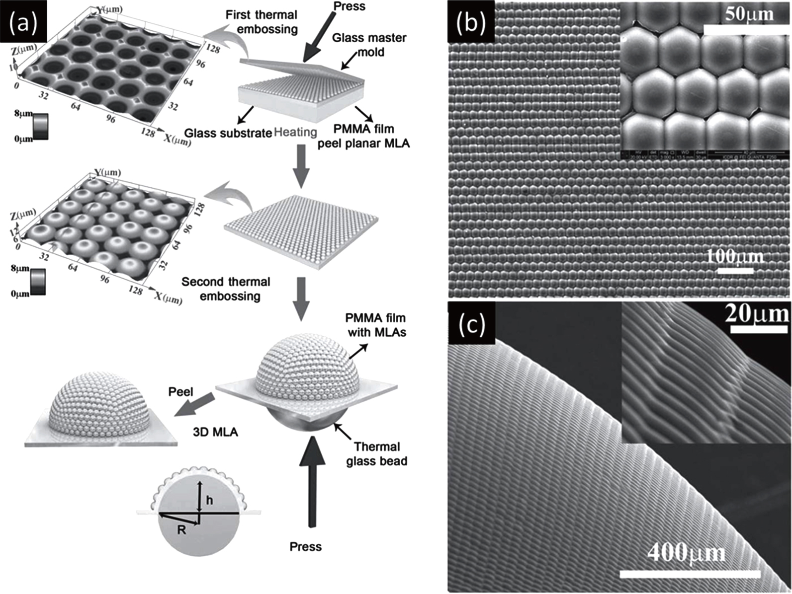
Fig. 4. Microfabrication of artificial compound eyes through double thermal molding. (a) Schematic of the fabrication process consisting of a combination of FsLMF, chemical etching, and thermal molding. (b) Top-view SEM image of the fabricated compound eyes; the inset shows the densely packed local convex microlenses. (c) Side-view SEM image of the macroscopic profile of the artificial compound eyes; the inset shows the microscopic convex profile of the microlenses.[26]

Another strategy for fast 3D microfabrications on curved surfaces is to use molding. In this strategy, a mold with concave microlens arrays on its curved inner surface needs to be pre-fabricated by EAFLM. An artificial compound eye structure can be then simply molded with soft materials such as polydimethylsiloxane (PDMS), which acquires the reverse structure of the inner-curved mold. Figures 5(a)5(d) show the processing flow diagram of the molding-enabled artificial compound eyes. The fabrication of the mold with concave microlens arrays was a wet-etching-based EAFLM on its curved inner surface. A 3D manipulation of the laser focus was inevitably needed during the femtosecond-laser seeding along the curved inner surface of the mold substrate. Instead of the rotating-stage control, a tilting-substrate control was performed as a simplified z-axis manipulation of the laser focus when the seeding location was shifted by a varied z-coordinate. This was realized by manually tilting the substrate by a corresponding angle. Together with the xy stage manipulation, laser seeding along the inner curved surface can be performed. The mold base used in Fig. 5(a) was a plano-concave lens (K-9 glass, diameter: 6 mm). After the chemical etching in Fig. 5(b), a glass mold with concave microlens array structures was obtained. PDMS source material was then poured inside and molded to obtain the reverse structure of the glass mold, as shown in Figs. 5(c) and 5(d). The macroscopic and microscopic morphologies of the PDMS compound eyes are shown in Figs. 5(e) and 5(f), respectively. The molded compound eye structure possesses a curved macroscopic surface, very similar to that of the natural eye structure, with a large number of ommatidia (3000). The diameters of the ommatidia are in the range of 93.18–96.18 μm, with an average sag height of 4.58 μm. The average deformation ratio of the ommatidia is estimated to be 2.96% with respect to the diameter, suggesting an acceptable fabrication fidelity. This deformation can be attributed to the z-axis laser focus manipulation by simply tilting the substrate. As the femtosecond laser pulse energy has a Gaussian distribution, the exposure lopsidedness would increase with the tilting angle of the substrate.[34]

Fig. 5. (color online) Microfabrication of artificial compound eyes through molding. (a)–(d) Schematic of the fabrication process, including (a) point-by-point femtosecond-laser seeding along the crater mold, (b) wet etching of concave microlens arrays, (c) PDMS injection and solidification, and (d) mold peeling off and formation of the compound eye structure. (e) and (f) SEM images of the artificial compound eye structure at a tilting angle of 45°.[34]
4. Conclusion and perspectives

The EAFLM has been advanced by a flexible combination of the core laser direct-writing and etching (as well as other techniques). With the help of etching (wet or dry), the 3D fabrications of complex array structures can be accelerated. The use of dry etching instead of chemical etching can avoid the post-etching effect and provide higher processing precision and integration compatibility. Conventional prototyping approaches (molding and thermal embossing) have also been included in EAFLM, helping realize fast 3D microfabrications on curved surfaces. Optical modulations, such as the single-pulse laser seeding, offer larger opportunities to further increase the fabrication efficiency. Moreover, such modulations advance the laser patterning step of EAFLM and make the array structures highly designable. They are very promising for the next-generation of micro-optic devices; therefore, it is of significance to perform further investigations. We believe that with the progress of the multi-technique-based EAFLM, more functional structures, in addition to compound eyes, can be realized with high structure designability and material-processing ability.

Reference
[1] Zhang Y L Chen Q D Xia H Sun H B 2010 Nano Today 5 435
[2] Han Y H Li Y Zhao X L Qu S L 2014 Chin. Phys. 23 094209
[3] Jin W Bi W H Fu G W 2017 Chin. Phys. 26 100702
[4] Ma L H Han W H Wang H Lyu Q F Zhang W Yang X Yang F H 2016 Chin. Phys. 25 068103
[5] Ma L H Han W H Wang H Yang X Yang F H 2015 Chin. Phys. 24 128101
[6] Xu C C Jiang L Leng N Liu P J 2013 Chin. Phys. 22 045203
[7] Cumming B P Schroder-Turk G E Debbarma S Gu M 2017 Light: Science & Applications 6 e16192
[8] Malinauskas M Zukauskas A Hasegawa S Hayasaki Y Mizeikis V Buividas R Juodkazis S 2016 Light: Science & Applications 5 e16133
[9] Ni J Wang C Zhang C Hu Y Yang L Lao Z Xu B Li J Wu D Chu J 2017 Light: Science & Applications 6 e17011
[10] Siegle T Schierle S Kraemmer S Richter B Wondimu S F Schuch P Koos C Kalt H 2017 Light: Science & Applications 6 e16224
[11] Wang L Chen Q D Cao X W Buividas R Wang X Juodkazis S Sun H B 2017 Light: Science & Applications 6 e17112
[12] Liu D X Sun Y L Dong W F Yang R Z Chen Q D Sun H B 2014 Laser & Photon. Rev. 8 882
[13] Wang L Wang H Y Wei H T Zhang H Chen Q D Xu H L Han W Yang B Sun H B 2014 Advanced Energy Mater. 4 1301882
[14] Xu H Cheng Y Chin S L Sun H B 2015 Laser & Photon. Rev. 9 275
[15] Turner M D Saba M Zhang Q Cumming B P Schroeder-Turk G E Gu M 2013 Nat. Photon. 7 801
[16] Oktem B Pavlov I Ilday S Kalaycioglu H Rybak A Yavas S Erdogan M Ilday F O 2013 Nat. Photon. 7 897
[17] Blasco E Mueller J Mueller P Trouillet V Schoen M Scherer T Barner-Kowollik C Wegener M 2016 Adv. Mater. 28 3592
[18] Sun Y L Li Q Sun S M Huang J C Zheng B Y Chen Q D Shao Z Z Sun H B 2015 Nat. Commun. 6 8612
[19] Son Y Yeo J Moon H Lim T W Hong S Nam K H Yoo S Grigoropoulos C P Yang D Y Ko S H 2011 Adv. Mater. 23 3176
[20] Seet K K Mizeikis V Matsuo S Juodkazis S Misawa H 2005 Adv. Mater. 17 541
[21] Kawata S Sun H B Tanaka T Takada K 2001 Nature 412 697
[22] Han D D Zhang Y L Ma J N Liu Y Q Han B Sun H B 2016 Adv. Mater. 28 8328
[23] Wang W Liu Y Q Liu Y Han B Wang H Han D D Wang J N Zhang Y L Sun H B 2017 Advanced Funct. Mater. 27 1702946
[24] Pan A Gao B Chen T Si J Li C Chen F Hou X 2014 Opt. Express 22 15245
[25] Wang L Chen Q D Yang R Xu B B Wang H Y Yang H Huo C S Sun H B Tu H L 2014 Appl. Phys. Lett. 104 031904
[26] Deng Z Chen F Yang Q Bian H Du G Yong J Shan C Hou X 2016 Advanced Funct. Mater. 26 1995
[27] Hu Y Yang Q Chen F Bian H Deng Z Du G Si J Yun F Hou X 2014 Appl. Surf. Sci. 292 285
[28] Deng Z Yang Q Chen F Meng X Bian H Yong J Shan C Hou X 2015 Opt. Lett. 40 1928
[29] Meng X Chen F Yang Q Bian H Du G Hou X 2015 Appl. Phys. 121 157
[30] Liu X Q Chen Q D Guan K M Ma Z C Yu Y H Li Q K Tian Z N Sun H B 2017 Laser & Photon. Rev. 11 1600115
[31] Cao X W Chen Q D Zhang L Tian Z N Li Q K Wang L Juodkazis S Sun H B 2018 Opt. Lett. 43 831
[32] Jeong K H Kim J Lee L P 2006 Science 312 557
[33] Huang C C Wu X Liu H Aldalali B Rogers J A Jiang H 2014 Small 10 3050
[34] Bian H Wei Y Yang Q Chen F Zhang F Du G Yong J Hou X 2016 Appl. Phys. Lett. 109 221109