
Growth and transport properties of topological insulator Bi2Se3 thin film on a ferromagnetic insulating substrate
Cite this Article
Zhu Shanna, Shi Gang, Zhao Peng, Meng Dechao, Liang Genhao, Zhai Xiaofang, Lu Yalin, Li Yongqing, Chen Lan, Wu Kehui. Growth and transport properties of topological insulator Bi2Se3 thin film on a ferromagnetic insulating substrate. Chinese Physics B, 2018, 27(7): 076801 
Permissions
Growth and transport properties of topological insulator Bi2Se3 thin film on a ferromagnetic insulating substrate
† Corresponding author. E-mail:
Project supported by the National Key R&D Program of China (Grant Nos. 2016YFA0300904 and 2016YFA0202301), the National Natural Science Foundation of China (Grant Nos. 11334011, 11674366, 11674368, and 11761141013), and the Strategic Priority Research Program of the Chinese Academy of Sciences (Grant Nos. XDB07010200 and XDPB06).
Abstract
Exchange coupling between topological insulator and ferromagnetic insulator through proximity effect is strongly attractive for both fundamental physics and technological applications. Here we report a comprehensive investigation on the growth behaviors of prototype topological insulator Bi2Se3 thin film on a single-crystalline LaCoO3 thin film on SrTiO3 substrate, which is a strain-induced ferromagnetic insulator. Different from the growth on other substrates, the Bi2Se3 films with highest quality on LaCoO3 favor a relatively low substrate temperature during growth. As a result, an inverse dependence of carrier mobility with the substrate temperature is found. Moreover, the magnetoresistance and coherence length of weak antilocalization also have a similar inverse dependence with the substrate temperature, as revealed by the magnetotransport measurements. Our experiments elucidate the special behaviors in Bi2Se3/LaCoO3 heterostructures, which provide a good platform for exploring related novel quantum phenomena, and are inspiring for device applications.
Keyword:topological insulator;ferromagnetic insulator;molecular beam epitaxy;magnetotransport properties
1. Introduction
The discovery of three-dimensional (3D) topological insulators (TIs) has attracted much attention in recent years due to their rich physics and promising applications in electronic and spintronic devices.[1–9] The exotic gapless surface states of TIs are protected by time-reversal symmetry (TRS), with locked spin-momentum which is immune to backscattering. On the other hand, the breaking of TRS will open up a gap in the Dirac surface states of TIs, leading to a massive Dirac fermion state which can give rise to many novel phenomena.[10–15] Introducing ferromagnetism into TIs through proximity effect with a ferromagnetic insulator (FMI) is an effective way to break the TRS, and it avoids bringing extra impurities compared with doping method.[16–27]
The prototype topological insulator, Bi2Se3, is a layered material with relatively large bulk energy gap among 3D TIs.[3,4] Experiments on the growth of Bi2Se3 thin films on different kinds of substrates have been reported, including Si(111), GaAs(111), graphene, SrTiO3(111), Al2O3(0001), and so on.[28–33] However, experiments on insulating ferromagnetic substrates are limited to a few kinds of materials, since the existing FMIs are very scarce in nature.[34] So far, the commonly used FMIs mostly possess low-symmetry structures associated with a poor growth quality, and the few known high-symmetry materials either have very low Curie temperatures (≤ 17 K), or require chemical doping of an otherwise antiferromagnetic matrix.[35]
LaCoO3 (LCO) single-crystalline thin film under tensile strain is a newly reported high-temperature perovskite ferromagnetic insulator.[35–38] The tensile-strained LaCoO3 film is shown to be a rare undoped high-symmetry FMI with a remarkably high TC of up to 85 K. Both experiments and first-principles calculations demonstrate tensile-strain-induced ferromagnetism due to the spin-state transition of Co3+ ion, which does not exist in bulk LaCoO3. More importantly, the strained LaCoO3 thin film can be prepared epitaxially on substrate such as the SrTiO3 (STO) with an atomically flat surface,[35] which is crucial for growing high-quality Bi2Se3 thin films onto it. Recently, we have found ferromagnetism in the Bi2Se3 film grown on LaCoO3/SrTiO3 by the proximity effect, implying that this system would be a promising platform for studying novel transport phenomena in TI/ferromagnetic structures.[39]
In this work, we systematically studied the growth behaviors of topological insulator Bi2Se3 thin films on LaCoO3/SrTiO3 by molecular beam epitaxy (MBE). We find that the optimal condition for Bi2Se3 to grow on LCO/STO is at a much lower substrate temperature, around 150 °C, as compared with the optimal temperature on bare STO. The thus obtained Bi2Se3 thin films display a well-organized morphology and high carrier mobility, similar to those grown on bare STO substrates at higher temperature. While at higher growth temperatures, Bi2Se3 films on LCO exhibit disordered film morphology and decreased carrier mobility. The magnetoresistance and characteristic weak antilocalization effect are also reduced at higher growth temperatures. These unusual behaviors may be attributed to the subtle strain stress and large thermal-expansion coefficient of LCO. Our exploration and realization of the Bi2Se3/LCO heterostructure will be promising for developing versatile spintronic device applications.
2. Experimental methods
2.1. Sample growth
The growth of Bi2Se3 thin films was carried out by a home-made MBE system in an ultrahigh vacuum (UHV) chamber with a base pressure lower than 2.0 × 10⁻¹⁰ Torr, equipped with reflection high-energy electron diffraction (RHEED) facility. As-prepared LCO single-crystalline thin films on (001)-oriented STO substrates were transferred into the UHV chamber and were degassed at 300 °C for about one hour before growth. High-purity Bi (99.997%) and Se (99.999%) sources were co-evaporated from the standard Knudsen cells, and deposited onto the surface of LCO, which was kept at a certain temperature during growth. The fluxes of Bi and Se were calibrated by a quartz crystal microbalance thickness monitor, and a high Se/Bi flux ratio of 10/1 was used in order to reduce the amount of Se vacancies. The typical growth rate of Bi2Se3 thin films used in this work was about 0.3 nm per minute. In-situ real-time RHEED was performed to monitor the growth dynamics during the whole process. For comparison, Bi2Se3 films were also grown on as-treated bare STO (001) substrates with the same procedures as that on LCO/STO.
2.2. Characterization
In-situ RHEED patterns were recorded during the film growth process to identify the film quality. Crystal structures of films were measured by x-ray diffraction (XRD) using a single crystal x-ray diffractometer (PANalytical) with Cu Kα1 radiation of wavelength 1.5406 Å in the ω–2θ scan. The surface morphologies of Bi2Se3 films were characterized by an atomic force microscope (AFM) in tapping mode.
Low-temperature electrical transport measurements were conducted in a helium cryostat system where a superconducting magnet was equipped, with temperature down to ∼1.7 K and magnetic field up to ±9 T. The Bi2Se3 films on LCO/STO were patterned into Hall bar geometry with a channel width of about 500 μm. The applied current was along the channel (denoted by x axis) and magnetic field applied in the perpendicular direction (z axis). Several batches of samples grown at different conditions were tested, and the typical results will be shown below. We also carried out transport measurements of the Bi2Se3 films grown on STO, to provide a reference data on non-magnetic substrates.
3. Results and discussion
where ψ(x) is the digamma function,
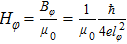
is the dephasing magnetic field, and lφ is the phase coherence length. The coefficient α = 0.5 is used for a system with single coherent channel, which is also expected for the electron transport on one surface of a 3D TI with a single Dirac cone.[41,42]
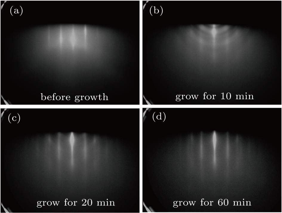
Figure
 | Fig. 1. RHEED patterns recorded during the deposition of Bi2Se3 film on LaCoO3 substrate. (a) The surface of LaCoO3 thin film after degassing, and before the Bi2Se3 film growth. (b), (c), and (d) were taken when the Bi2Se3 film has grown for 10 min (3 QL), 20 min (6 QL), and 60 min (18 QL), respectively. |
High quality of the Bi2Se3 film is also verified by XRD measurement on Bi2Se3/LCO samples. In Fig.
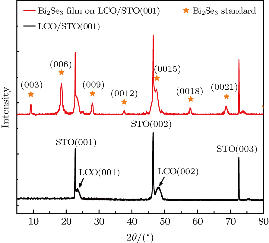 | Fig. 2. X-ray diffraction spectrum of a 20 QL Bi2Se3 film on LaCoO3/SrTiO3(001) (red line) and the data of an as-prepared LaCoO3 film on SrTiO3(001) substrate (black line) for comparison. The standard data (ICSD card) of Bi2Se3 single crystal is also shown (marked as orange star symbols) as a reference. |
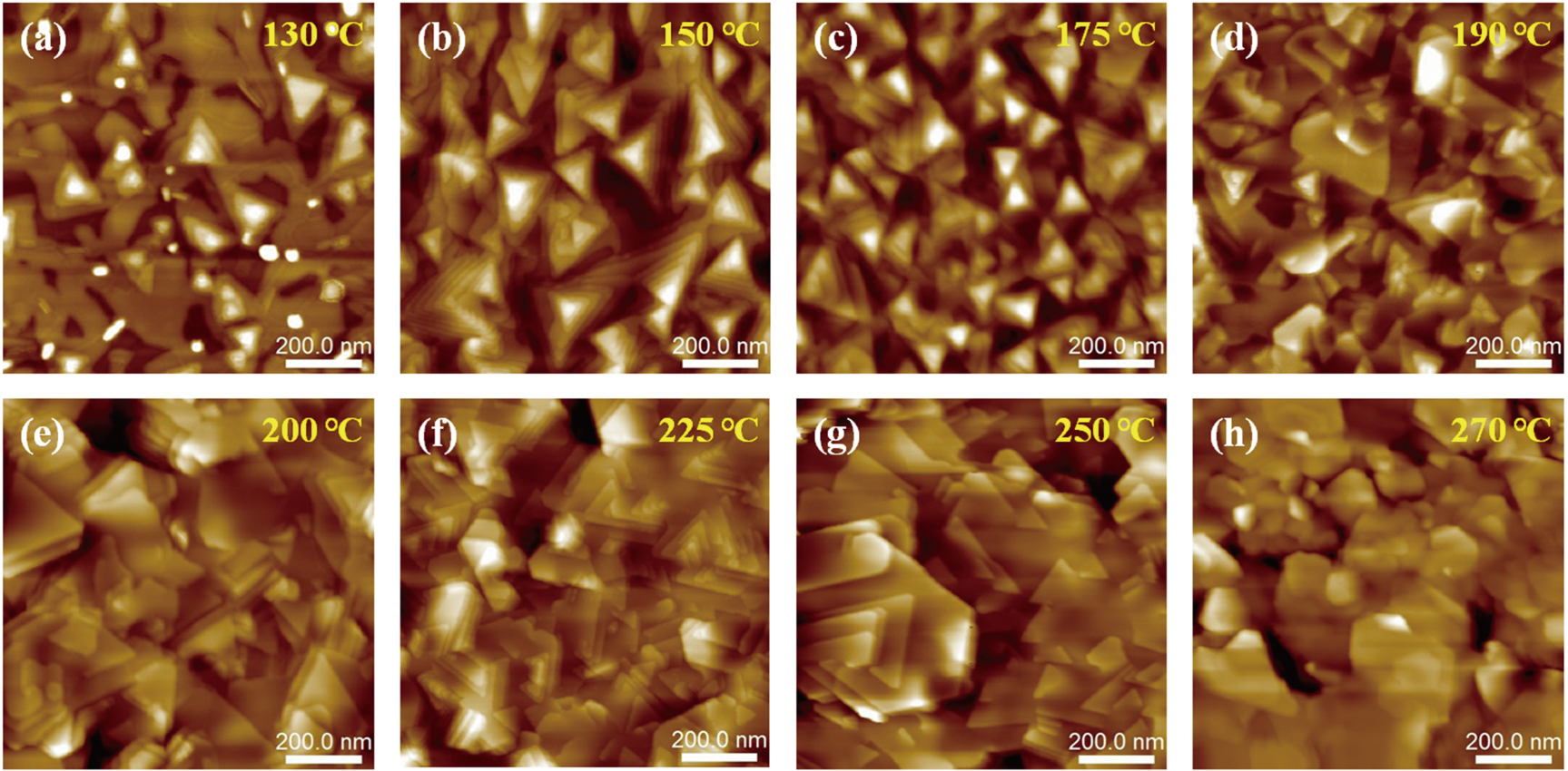
To investigate the influence of different substrate temperatures during growth on the film morphology, we scanned the surface of the Bi2Se3 films through AFM technique. Figure
 | Fig. 3. AFM images (size: 1 μm×1 μm) of a series of Bi2Se3 films grown on LaCoO3/SrTiO3(001) substrate at different substrate temperatures: (a) 130 °C, (b) 150 °C, (c) 175 °C, (d) 190 °C, (e) 200 °C, (f) 225 °C, (g) 250 °C, and (h) 270 °C. All the films have been grown for 60 min. |
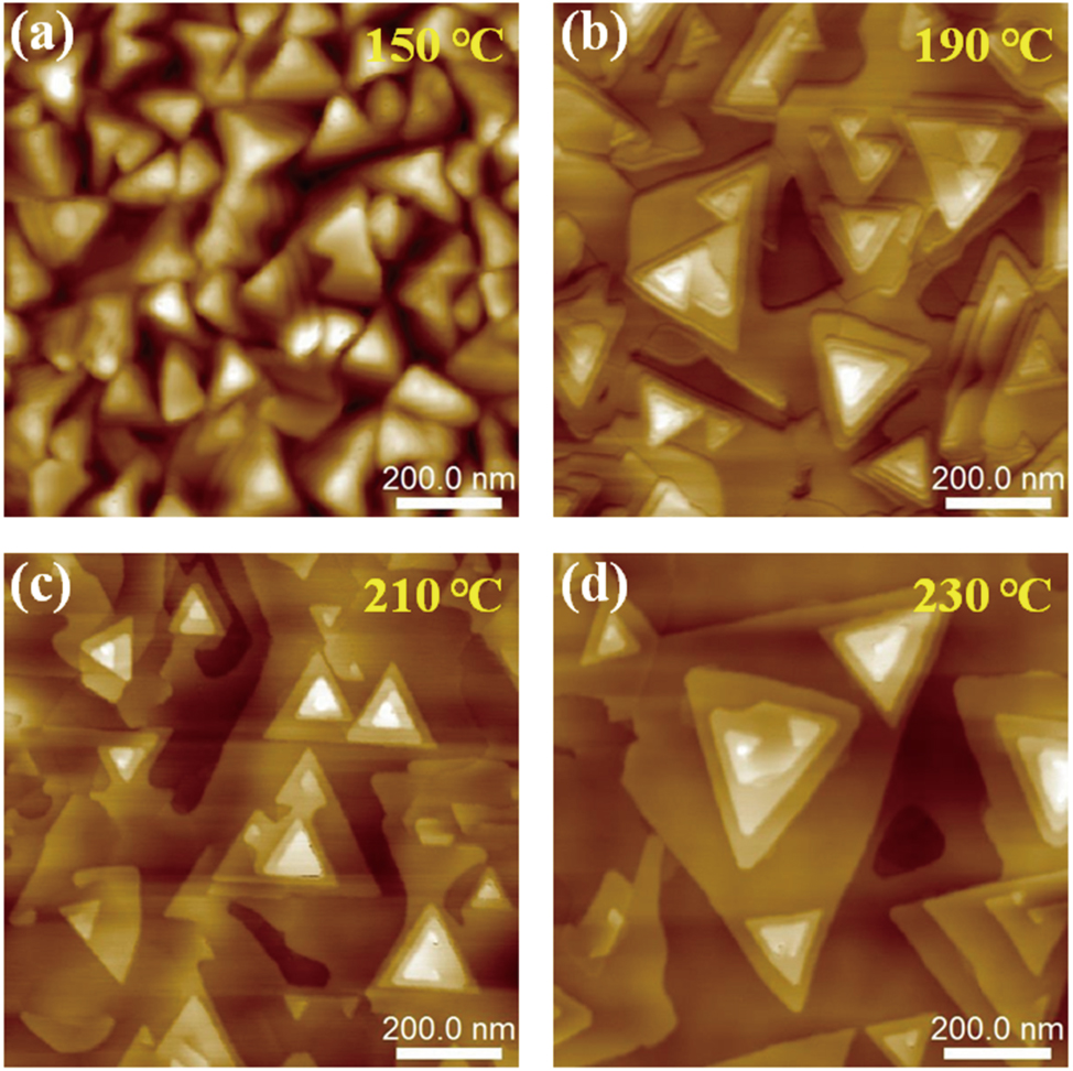
For comparison, the morphologies of Bi2Se3 films on pure STO(001) substrates were investigated under the same growth conditions. As shown in Fig.
 | Fig. 4. AFM images (size: 1 μm × 1 μm) of Bi2Se3 film grown on SrTiO3(001) substrate at different substrate temperatures: (a) 150 °C, (b) 190 °C, (c) 210 °C, and (d) 230 °C. All the films have been grown for 60 min, under the same conditions as that in Fig. |
In general, Bi2Se3 thin films can be layer-by-layer grown on different kinds of substrates with even slight lattice mismatch, due to the van der Waals epitaxy. In these cases, including on the pure STO(001) substrate, Bi2Se3 thin film tends to have a smoother surface at a relatively higher temperature above 200 °C, which allows sufficient diffusion of the Bi and Se atoms.[30–33] While in the case of LCO/STO, higher substrate temperature seems to have a negative influence on the film quality of Bi2Se3. Compared with other substrates, LCO has a larger thermal-expansion coefficient.[36] The expanded lattice of underlying LCO layer and the accompanied influence on strain stress due to lattice mismatch becomes more obvious at high substrate temperature, which results in the disordered morphology of films. Therefore, by exploring a wide range of possible growth temperatures, we find that only at the relatively lower temperature can Bi2Se3 film be grown onto LCO/STO in free-standing QL-by-QL mode, as it does on other substrates.
For transport measurements, we chose a thickness of 20 QL for the Bi2Se3 films, which is well above the thickness threshold of 6 nm. Below this threshold, the top and bottom surface of Bi2Se3 may be coupled by quantum tunneling and lead to a hybridization gap near Dirac point, similar to the result brought by strong magnetic interaction.[40] In Fig.
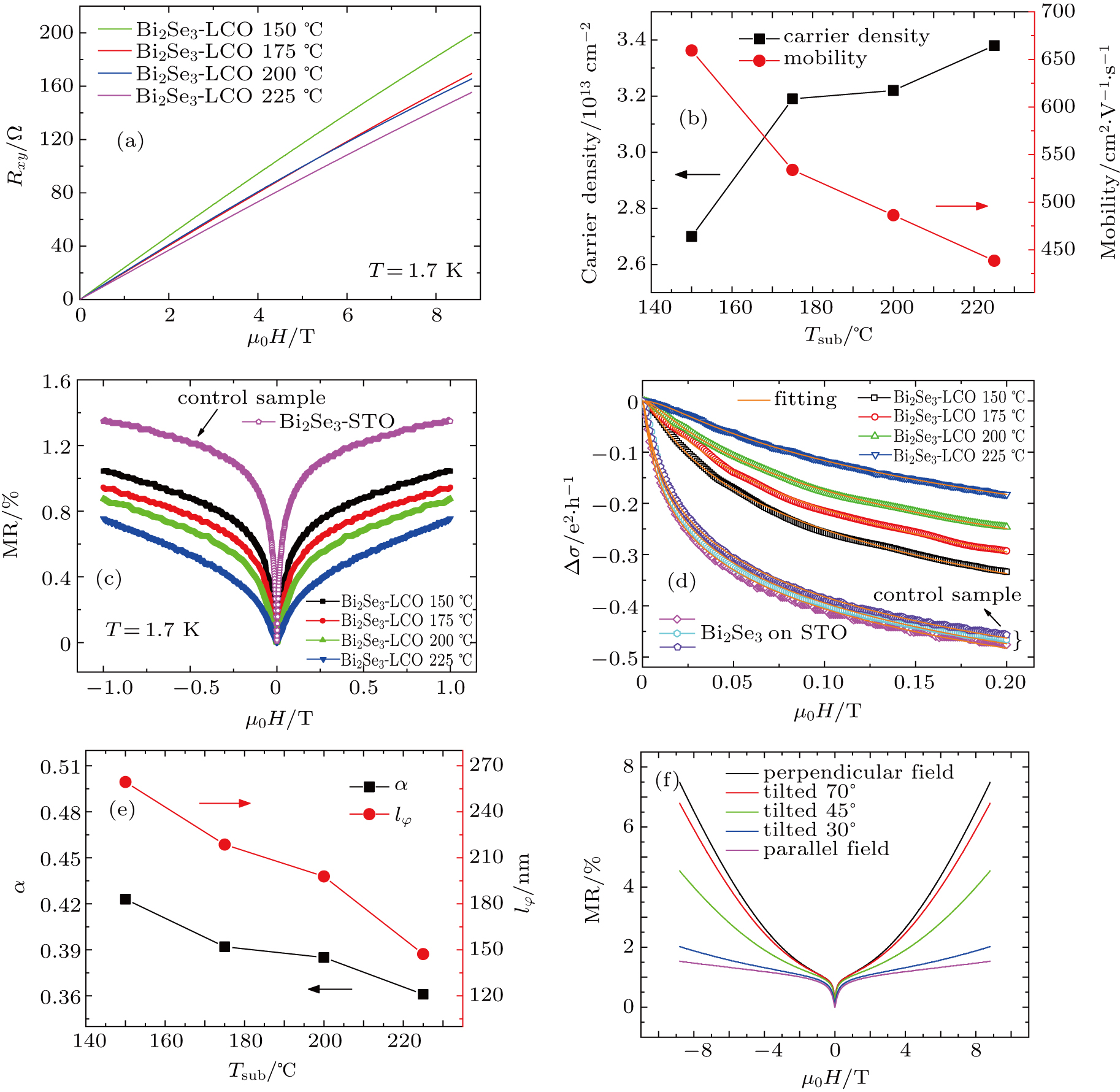
 | Fig. 5. Magnetotransport properties of the Bi2Se3/LCO heretostructure devices. All the data are measured at 1.7 K. (a) Hall resistance (Rxy) of several Bi2Se3/LCO samples as a function of the perpendicular magnetic field. (b) Initial carrier density (black squares) and carrier mobility (red circles) derived from several Bi2Se3/LCO samples grown at different substrate temperatures (denoted by Tsub) ranging from 150 °C to 225 °C. (c) Magnetoresistance (MR) measured in perpendicular magnetic field of four Bi2Se3/LCO samples (in solid symbols) grown at Tsub = 150 °C, 175 °C, 200 °C, 225 °C, respectively, and a control sample (in pink open symbol) of Bi2Se3/STO grown at Tsub = 150 °C. (d) Magnetoconductivity in low-field range of the corresponding samples in (c) as well as two additional curves of the Bi2Se3/STO control sample with Tsub = 150 °C at gate voltage 30 V and −100 V, respectively. The HLN fitting results of each curve are plotted in solid (orange) lines. (e) The fitting parameters of HLN equation for each Bi2Se3/LCO sample shown in (d). (f) MR of a typical Bi2Se3/LCO sample grown at optimal Tsub = 150 °C measured in tilted field. The tilted angle is defined as the angle between the applied magnetic field and the film plane. |
The initial carrier density and carrier mobility of four Bi2Se3/LCO samples grown at different substrate temperatures (Tsub) are plotted in Fig.
Figure
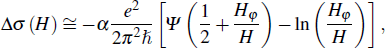
Further analysis of the WAL effect is carried out by a quantitative fitting of low-field magnetoconductance (MC) data. The magnetoconductivity is defined as Δσ(H) = σxx(H) − σxx(0), where the sheet conductance (σ) is calculated by the relation σxx = ρxx/(ρyx2 + ρxx2). As proposed in the literature,[41–46] the WAL quantum corrections to the low-field magnetoconductivity in the strong spin–orbit coupling (SOC) limit can be described by the Hikami–Larkin–Nagaoka (HLN) equation[47]
 |
As plotted in Fig.
Transport properties in the tilted magnetic field are also measured for the Bi2Se3/LCO samples, as shown in Fig.
The above data of magnetotransport measurements further indicate a crucial role played by the substrate temperature during growth, where the disorder arising from higher substrate temperature is proven to be disadvantageous for the transport properties of samples. These results are in consistence with the analysis of film morphology, and corroborate the conclusion that low substrate temperature is favorable for the growth of Bi2Se3/LCO.
4. Conclusion
In conclusion, we have performed a systematic investigation on the growth behaviors of epitaxial Bi2Se3 thin films on a ferromagnetic insulating LCO/STO substrate, which forms a new TI/FMI heterostructure. The Bi2Se3 films with highly crystalline structure and well-ordered surface are obtained at a relatively low substrate temperature of 150 °C during growth. Transport measurement confirms high carrier mobility in the sample grown at optimal conditions. An unusual dependence of film morphology and transport properties on the growth temperatures are observed, and can be attributed to the large thermal-expansion coefficient of LCO substrate and the increased strain stress at the interface at high substrate temperature. Our results and methodology of fabricating such high-quality TI/FMI heterostructure provide not only a platform for investigating the proximity-induced magnetism in TIs, but a versatile approach to explore the TI-based spintronic devices in applications.
Reference
| [1] | |
| [2] | |
| [3] | |
| [4] | |
| [5] | |
| [6] | |
| [7] | |
| [8] | |
| [9] | |
| [10] | |
| [11] | |
| [12] | |
| [13] | |
| [14] | |
| [15] | |
| [16] | |
| [17] | |
| [18] | |
| [19] | |
| [20] | |
| [21] | |
| [22] | |
| [23] | |
| [24] | |
| [25] | |
| [26] | |
| [27] | |
| [28] | |
| [29] | |
| [30] | |
| [31] | |
| [32] | |
| [33] | |
| [34] | |
| [35] | |
| [36] | |
| [37] | |
| [38] | |
| [39] | |
| [40] | |
| [41] | |
| [42] | |
| [43] | |
| [44] | |
| [45] | |
| [46] | |
| [47] | |
| [48] |