Enhancement of off-state characteristics in junctionless field effect transistor using a field plate*

Project supported by the National Natural Science Foundation of China (Grant No. 61704130), the Fundamental Research Funds for the Central Universities, China (Grant No. 20101166085) and the Opening Project of Key Laboratory of Microelectronic Devices & Integrated Technology from Institute of Microelectronics, Chinese Academy of Sciences (Grant No. 90109162905).

Wang Bin1, †, Zhang He-Ming2, Hu Hui-Yong2, Shi Xiao-Wei1
State Key Discipline Laboratory of Wide Bandgap Semiconductor Technology, School of Advanced Materials and Nanotechnology, Xidian University, Xi’an 710071, China
State Key Discipline Laboratory of Wide Bandgap Semiconductor Technology, School of Microelectronics, Xidian University, Xi’an 710071, China


† Corresponding author. E-mail: wbin@xidian.edu.cn

Project supported by the National Natural Science Foundation of China (Grant No. 61704130), the Fundamental Research Funds for the Central Universities, China (Grant No. 20101166085) and the Opening Project of Key Laboratory of Microelectronic Devices & Integrated Technology from Institute of Microelectronics, Chinese Academy of Sciences (Grant No. 90109162905).

Abstract

In this paper, a novel junctionless field effect transistor (JLFET) is proposed. In the presence of a field plate between gate and drain, the gate-induced drain leakage (GIDL) effect is suppressed due to the decrease of lateral band-to-band tunneling probability. Thus, the off-state current Ioff, which is mainly provided by the GIDL current, is reduced. Sentaurus simulation shows that the Ioff of the new optimized JLFET is reduced by ∼ 2 orders and its sub-threshold swing can reach 76.8 mV/decade with little influence on its on-state current Ion, so its Ion/Ioff ratio is improved by 2 orders of magnitude compared with that of the normal JLFET. Optimization of device parameters such as Φfps (the work difference between field plate and substrate) and LFP (the length of field plate), is also discussed in detail.

1. Introduction

In the down-scaling approach, conventional Si metallic-oxide semiconductor field-effect transistors (MOSFETs) are approaching towards the end of the technology roadmap.[13] One of the main reasons is that the rapid down-scaling of conventional bulk MOSFETs below 45 nm requires an ultrasteep doping profile at the metallurgical junction and a high thermal budget corresponding to the post-anneal dopant activation, which leads to extreme troubles in device fabrication.[4,5] To overcome this limitation, various alternative devices are being proposed, and a new class of field effect device called the junctionless field-effect transistor (JLFET) has attract lots of research attention in recent years.[614]

The basic structure of a JLFET consists of a uniformly highly doped silicon channel controlled by at least an on gate electrode. Unlike “regular” junction-based FETs, in JLFET, both the source and the drain have the same type of doping as the channel, and there is no pn junction. The principle of JLFET operation is also quite different as it counts on majority carriers instead of minority carriers. Moreover, the current flows mainly in the volume and is no longer confined at the Si/SiO2 interface. Based on these specific conduction mechanisms, JLFET has a large on-state current Ion and an excellent drive capability, which could be improved by increasing the doping concentration.

However, high doping will increase not only the on-state current Ion but also the off-state current Ioff, thus affecting the ratio of Ion over Ioff.[1517] Furthermore, above certain doping levels, the device could not be switched off even at the off state of the device. As in conventional MOSFET, the off-state current Ioff in JLFET is mainly caused by the gate-induced drain leakage (GIDL) effect at the gate edge between gate and drain.[1820] Since the efficient gate control over the channel region leads to a considerable overlap of the valence band with the conduction band at the channel–drain interface, a lateral band-to-band tunneling (L-BTBT) of electrons from the channel region to the drain region in the off-state (VGS = 0 V), which is a dominant mechanism for GIDL in JLFET. In order to reduce Ioff, several device structures have been designed, such as JLFET with dielectric pocket double gate,[21] JLFET with hybrid channel,[22] JLFET with core-shell architecture,[23] etc.

In this paper, we propose a novel JFELT with field plate structure to reduce the high field effect at the gate edge, finally suppressing the GIDL effect and Ioff. The TCAD simulation indicates that Ioff of the new optimized JLFET is reduced by ∼ 2 orders and its sub-threshold swing can reach 76.8 mV/decade with little affection on its Ion, so its Ion/Ioff ratio is improved by 2 orders of magnitude over the normal JLFET. Optimization of device parameters such as Φfps (the work difference between field plate and Si) and LFP (the length of field plate) is also discussed in detail.

2. Device structure and simulation parameters

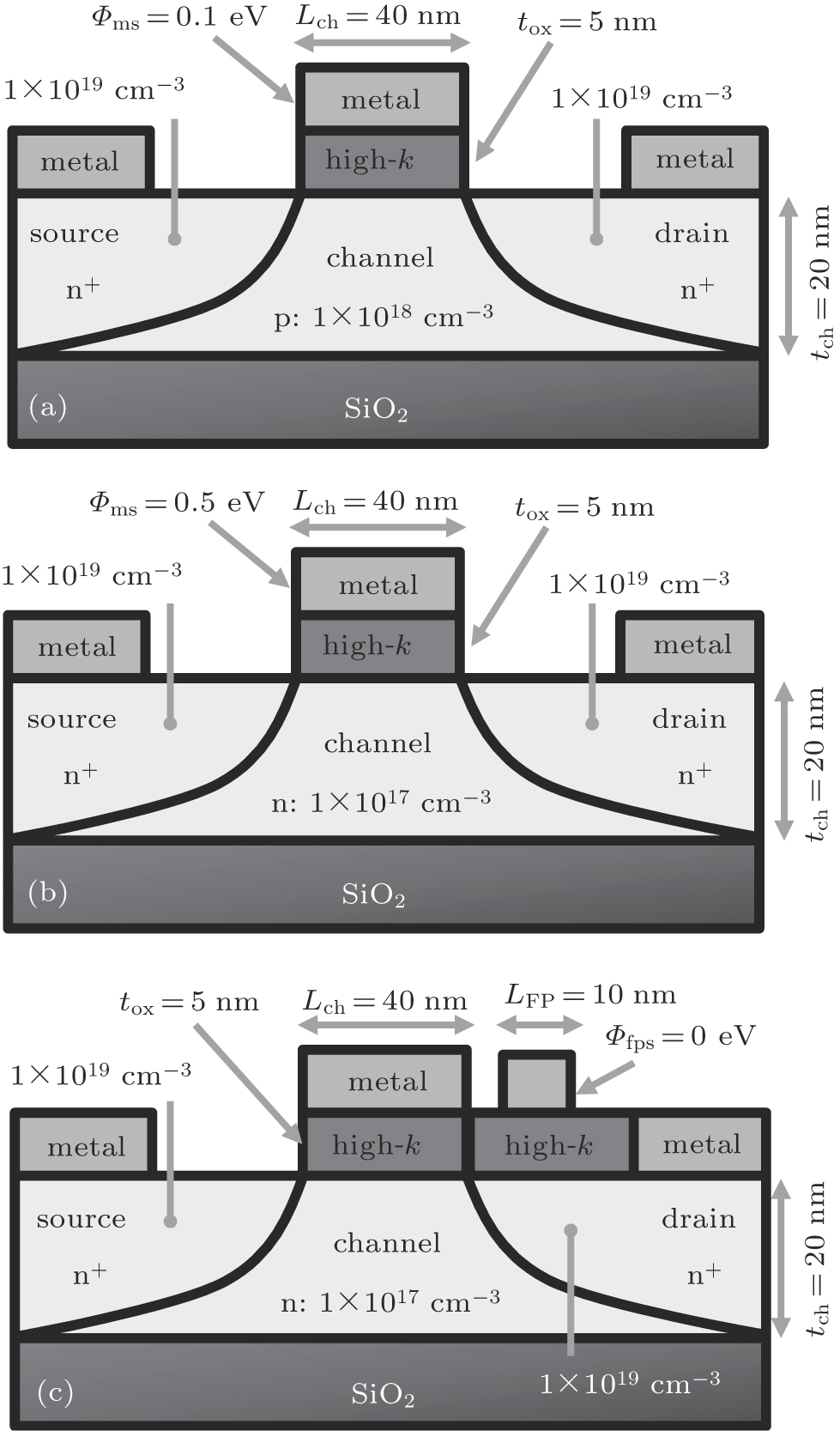
The schematic views of the conventional MOSFET, the normal JLFET, and the novel JFLET (FP JLFET) are shown in Figs. 1(a)1(c), respectively. The length of the gate, length of the field plate, thickness of the oxide, and thickness of channel are denoted as Lch, LFP, tox, and tch. The channels of the JLFET and the FP JLFET are lightly doped (1 × 1017 cm−3), the drain and source are heavily doped (1 × 1019 cm−3). The metal of the gate electrode is Cr/Au for ensuring the device to be fully depleted at VGS = 0 V. The high-k material of HfO2 is used as gate dielectric and field plate dielectric. The field plate in FP JLET shown in Fig. 1(c) is located between gate and drain electrodes. In order not to affect the device size, the length of field plate LFP cannot be longer than the distance between gate and drain electrodes.

Fig. 1. Cross sections of (a) conventional MOSFET, (b) normal JLFET, and (c) FP JLFET.

Sentaurus TCAD was used to perform the device simulations. The field-dependent and doping dependent mobility degradations were considered using the Philips unified mobility model and Lombardi mobility model. Bandgap narrowing, Shockley–Read–Hall, the Auger recombination model, and Fermi–Dirac statistics were also involved. A nonlocal BTBT model was used to account for the lateral tunneling of the GIDL effect. A temperature of 300 K was employed in simulations.

3. Simulation results and discussion

Figure 2 shows the electric field underneath the gate of normal JLFET and FP JLFET. To make a comparison, the electric field curve of conventional MOSFET is also given in this experiment. Owing to the capacitive coupling effect,[2426] the peak of the electric field at the edge of the gate decreases significantly and a relatively low peak of electric field is created at the edge of the field plate, thus leading to a larger tunneling width in FP JLFET as shown in Fig. 3.

Fig. 2. (color online) Plots of electric field along the vertical direction of the channel underneath the gate in the off-state (VDS = 1.0 V, VGS = 0 V), with inset showing GBTBT near the gate edge.
Fig. 3. (color online) Energy bands along the parallel directions of channels of JLFET and FP JLFET underneath the gate, in off-state (VDS = 1.0 V, VGS = 0 V).

Figure 3 shows a comparison of energy band structure along the parallel channel direction between normal JLFET and FP JLFET at the surface. The EFp, Tw1, and Tw2 represent the Fermi energy level, and the tunneling width of normal JLFET and FP JLFET respectively. As discussed above, the electric field between gate and drain in FP JLFET is more uniform by employing the field plate structure, leading to the decrease of band bending of FP JLFET compared with that of JLFET. Therefore, Tw2 is larger than Tw1. An enhanced tunneling width leads to the decrease of the electrons tunneling from the channel region to the drain region, resulting in a significantly reduced BTBT generation rate in the new FP JLFET compared with that in the normal JLFET as shown in the inset of Fig. 2.

The transfer characteristics of the new FP JLFET and normal JLFET (VDS = 1 V) are shown in Fig. 4. To show the advantages of FP JLFET more obviously, the IDVG curve of conventional MOSFET is also given in this experiment. We can observe that the off-state current Ioff of normal JLFET with the BTBT model increases more than 3 orders of magnitude (from 9.25 × 10⁻¹¹ A/μm to 5.7 × 10⁻⁷ A/μm), indicating that Ioff is mainly caused by the GIDL effect. With the field plate employment, the Ioff is drastically reduced in the FP JLFET by 2 orders of magnitude compared with that of normal JLFET, resulting in an improvement in its sub-threshold swing SS as shown in Fig. 4(b).

Fig. 4. (color online) (a) IDVG characteristics of conventional MOSFET, normal JLFET, and FP JLFET at VDS = 1.0 V. (b) Comparisons of Ion, Ioff, Ion/Ioff, and SS among conventional MOSFET, normal JLFET, and FP JLFET.

Also from Fig. 4, we can observe that the values of on-state current Ion of JLFET and FP JLFET are at the same level, since the field plate structure has little effect on the on-state current Ion, which is mainly composed of the drifting current of majority carriers. Thus, the Ion/Ioff ratio of FP JLFET has a more apparent improvement than that of JLFET, almost being at the level of a conventional MOSFET and manifesting the advantages of FP JLFET.

To study the influence of Φfps on GIDL and the electrical characteristics of FP JLFET, the IDVG curves with various values of Φfps were simulated as shown in Figs. 5(a) and 5(b). Since the increase of Φfps enhances the repelling effect on electrons, the electron density decreases at the surface of FP JLFET with Φfps increasing, finally reducing the on state current Ion of the device.

Fig. 5. (color online) (a) IDVG characteristics of the FP JLFET with various values of Φfps (Φfps = −0.4 eV, −0.2 eV, 0.0 eV, 0.2 eV, 0.4 eV, 0.6 eV) at VDS = 1.0 V. (b) Comparisons of Ion, Ioff, Ion/Ioff, and SS of the FP JLFET with various values of Φfps.

Also from Fig. 5, we can see that Ioff first decreases and then increases with Φfps increasing. As Φfps increases from −0.4 eV to 0.0 eV, Ioff decreases from 7.71 × 10⁻⁹ A/μm to 2.81 × 10⁻¹⁰ A/μm, and as Φfps increases from 0.0 eV to 0.6 eV, Ioff increases about 3 orders of magnitude (from 2.81 × 10⁻¹⁰ A/μm to 1.96 × 10⁻⁷ A/μm). Therefore, the Ion/Ioff ratio first increases and then decreases with Φfps increasing, and the optimal Ion/Ioff and SS are achieved when Φfps = 0.0 eV as shown in Fig. 5(b).

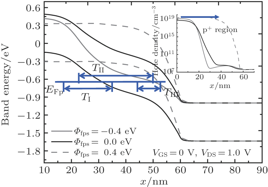
To understand the phenomenon above, the energy bands along the parallel direction of the FP JLFET with various values of Φfps (Φfps = −0.4 eV, 0.0 eV, and 0.4 eV) in the off-state are examined as shown in Fig. 6. TI, TII, and TIII are the width of the tunneling barrier of the GIDL effect with Φfps = −0.4 eV, 0.0 eV, and 0.4 eV, respectively. It is obvious that the TII is largest, which ensures the optimal value of off state current Ioff. Besides, the position of the tunneling barrier shifts from gate edge to field plate edge with Φfps increasing. The reason is as follows. The density of electrons under the field plate decreases with Φfps increasing and finally the holes will be accumulated at the surface under the field plate, resulting in the p+ region extending from the gate edge to the floating plate edge, which is shown in the inset of Fig. 6. Thus, the tunneling position shifts. Owing to the two reasons discussed above, the optical value for Φfps is chosen to be 0 eV in our simulations.

Fig. 6. (color online) Energy bands along the parallel direction of FP JLFET with various values of Φfps (Φfps = −0.4 eV, 0.0 eV, 0.4 eV underneath the gate, in the off-state (VDS = 1.0 V, VGS = 0 V), with inset showing hole density along the parallel direction.

Another important parameter affecting the off-state current of the FP JLFET is LFP. Figure 7 shows the IDVG curves of FP JLFET with LFP values of 5 nm, 10 nm, 25 nm, 20 nm, and 25 nm. The off-state current Ioff decreases more than 2 orders of magnitude as LFP increases from 5 nm to 25 nm, resulting in a significant improvement in Ion/Ioff and SS. The reason is shown in Fig. 8. Figure 8 gives the energy band along the parallel direction of the FP JLFET with various values of LFP underneath the gate in the off-state. It is shown obviously that the tunneling width is enlarged with the LFP increasing and reaches its largest value at LFP = 25 nm, thus the BTBT tunneling and GIDL effect are restricted, reducing the Ioff significantly.

Fig. 7. (color online) (a) IDVG characteristic curves of FP JLFET with various values of LFP at VDS = 1.0 V. (b) Comparisons of Ion, Ioff, Ion/Ioff, and SS of the FP JLFET with various values of LFP.
Fig. 8. (color online) Energy bands along the parallel direction of the FP JLFET with various values of LFP underneath the gate, in the off-state (VDS = 1.0 V, VGS = 0 V).
4. Conclusions

In this work, we have proposed a JLFET with a field plate for significantly improving the off-state performance. Using Sentaurus simulations, we demonstrate that the field plate in the new device can effectively broaden the tunneling barrier width at the drain-channel interface, resulting in the occurrence of insufficient band bending for L-BTBT and thus restricting the GIDL effect in the new JLFET. Therefore, the proposed device architecture provides the off-state current reduced by 2 orders of magnitude without deteriorating the on-state current, resulting in a significant Ion/Ioff ration enhancement compared with the scenario of the conventional JLFET. Our results may promote the experimental realization of this structure.

Reference
[1] Taur Y Chen H P Wang W Lo S H Wann C 2012 IEEE Trans. Electron Dev. 59 863
[2] Wang B Zhang H M Hu H Y Zhang Y M Zhou C Y Wang G Y Li Y C 2013 Chin. Phys. 22 028503
[3] Li Y C Zhang H M Zhang Y M Hu H Y Wang B Lou Y L Zhou C Y 2013 Chin. Phys. 22 038501
[4] Leung G Pan A Chi C 2015 IEEE Trans. Electron Dev. 62 3208
[5] Han M H Chang C Y Jhan Y R Wu J J Chen H B Cheng Y C Wu Y C 2013 IEEE Electron Dev. Lett. 34 157
[6] Li C Zhuang Y Q Zhang L Jin G 2014 Chin. Phys. 23 038502
[7] Migita S Morita Y Matsukawa T Masahara M Ota H 2014 IEEE Trans. Nanotechnol. 13 208
[8] Im K S Seo J H Yoon Y J Jiang Y I 2014 Jpn. J. Appl. Phys. 53 8130
[9] Li C Zhuang Y Q Zhang L Jin G 2014 Chin. Phys. 23 018501
[10] Jhan Y R Thirunavukkarasu V Wang C P Wu Y C 2015 IEEE Electron Dev. Lett. 36 654
[11] Gupta M Kranti A 2015 ECS Trans. 66 2285
[12] Wong I Chen Y T Huang S H Tu W H Chen Y S Liu C W 2015 IEEE Trans. Nanotechnol. 14 878
[13] Wang H Han W H Zhao X S Zhang W Lv Q F Ma L H Yang F H 2016 Chin. Phys. 25 0108102
[14] Liu F Y Liu H Z Liu B W Guo Y F 2016 Chin. Phys. 25 047305
[15] Lucian B Farzan J Didier B Jean-Michel S 2013 IEEE Trans. Electron Dev. 60 2080
[16] Shibir B Pranav K A Yogesh G Bahniman G 2015 Appl. Phys. 118 1527
[17] Shubham S Mamidala J K 2017 IEEE Trans. Electron Dev. 64 1330
[18] Shiromani B R Bahniman G 2015 RSC Adv. 5 59665
[19] Shubham S Mamidala J K 2016 IEEE Trans. Electron Dev. 63 4138
[20] Shubham S Mamidala J K 2017 IEEE Trans. Electron Dev. 64 2604
[21] Balraj S Deepti G Ekta G Sanjay K Kunal S Satyabrata J 2016 J. Comput. Electron. 15 502
[22] Mamidala J K Shubham S 2016 IEEE Trans. Electron Dev. 63 3250
[23] Shubham S Mamidala J K 2016 IEEE Trans. Electron Dev. 63 3790
[24] Mao W She W B Yang C Zhang J F Zheng X F Wang C Hao Y 2016 Chin. Phys. 25 017303
[25] Cheng K Hu S D Lei M Yuan Q Jiang Y Y Huang Y Yang D Lin Z Zhou X C Tang F 2017 Superlattices and Microstructures in press
[26] Liu S Y Ren X F Fang Y C Sun W F Su W Ma S L Lin F Liu Y W Sun G P 2017 IEEE Trans. Electron Dev. 64 3275