


Low specific on-resistance GaN-based vertical heterostructure field effect transistors with nonuniform doping superjunctions
Cite this Article
Mao Wei, Wang Hai-Yong, Shi Peng-Hao, Wang Xiao-Fei, Du Ming, Zheng Xue-Feng, Wang Chong, Ma Xiao-Hua, Zhang Jin-Cheng, Hao Yue. Low specific on-resistance GaN-based vertical heterostructure field effect transistors with nonuniform doping superjunctions. Chinese Physics B, 2018, 27(4): 047305 
Permissions
Low specific on-resistance GaN-based vertical heterostructure field effect transistors with nonuniform doping superjunctions
† Corresponding author. E-mail:
Abstract
A novel GaN-based vertical heterostructure field effect transistor (HFET) with nonuniform doping superjunctions (non-SJ HFET) is proposed and studied by Silvaco-ATLAS, for minimizing the specific on-resistance (RonA) at no expense of breakdown voltage (BV). The feature of non-SJ HFET lies in the nonuniform doping concentration from top to bottom in the n- and p-pillars, which is different from that of the conventional GaN-based vertical HFET with uniform doping superjunctions (un-SJ HFET). A physically intrinsic mechanism for the nonuniform doping superjunction (non-SJ) to further reduce RonA at no expense of BV is investigated and revealed in detail. The design, related to the structure parameters of non-SJ, is optimized to minimize the RonA on the basis of the same BV as that of un-SJ HFET. Optimized simulation results show that the reduction in RonA depends on the doping concentrations and thickness values of the light and heavy doping parts in non-SJ. The maximum reduction of more than 51% in RonA could be achieved with a BV of 1890 V. These results could demonstrate the superiority of non-SJ HFET in minimizing RonA and provide a useful reference for further developing the GaN-based vertical HFETs.
Keyword:;GaN-based vertical HFETs;;nonuniform doping superjunctions;;minimized specific on-resistance;;breakdown voltage;
1. Introduction
The desire for power electronic systems with increasingly excellent performances has been the catalyst for developing GaN-based power devices, in which the vertical GaN-based heterostructure field effect transistor (GaN-based V-HFET), as a kind of high-power switch device, has been attracting increasing attention. Compared with its lateral counterpart (GaN-based HEMT),[1–6] the GaN-based V-HFET has the superiorities, i.e., the reduced chip area, the packaging convenience and the suppression of current collapse,[7] which makes it significantly advantageous and perhaps the only topology choice for power conversions beyond 15 kW.[8] In a high power system, it has been one of the most important focuses to minimize the system power loss. Therefore, the reduction of the specific on-resistance in GaN-based V-HFET is strongly required to reduce the power device loss even at high frequency operation,[9] which depends on a better trade-off characteristic between breakdown voltage (BV) and specific on-resistance (RonA).
Recently, a great deal of effort has been made to develop the device structures and fabrication process for GaN-based V-HFETs. Many novel V-HFET structures have been proposed to further improve the trade-off between BV and RonA,[10–13] of which the GaN-based V-HFET with uniform doping superjunction (un-SJ HFET) could be considered as the most effective and promising candidate.[11] Furthermore, the successful applications of the etching technology, the regrowth technology and the implantation technology in the fabrication of GaN-based V-HFETs[7,8,14–16] have enhanced the possibility of realizing various novel vertical device structures. These advances are a great encouragement to the further study of GaN-based V-HFETs.
In this paper, a novel GaN-based V-HFET with nonuniform doping superjunction (non-SJ HFET) is presented and investigated. The study of this device emphasizes the further reduction in RonA with the same BV as that of the conventional un-SJ HFET. Compared with un-SJ HFET, the non-SJ HFET has an obvious feature that is the nonuniform doping superjunction (non-SJ) comprising nonuniform doping n- and p-pillars. Based on this, the specific on-resistance could be remarkably reduced without any loss of BV. Two-dimensional numerical simulation with Silvaco-ATLAS software is performed to reveal the intrinsic operation mechanism for the non-SJ by using the potential distributions, electric field distributions and current density distributions. The relationship among the RonA, the BV and the structure parameters of the non-SJ is studied systematically, aiming at optimizing the minimized RonA. These results are of importance for designing and further developing the GaN-based V-HFETs.
2. Device structures and physic models
Figure 


 | Fig. 1. (color online) Schematic structures for (a) non-SJ HFET and (b) un-SJ HFET. Lines A1A2 or B1B2 denote the vertical direction at the n-pillar/p-pillar junction or the middle of the device, respectively. |
| Table 1.
Main structure specifications for non-SJ HFET and un-SJ HFET. . |
Two-dimensional device simulations are performed by using the Silvaco-ATLAS. The polarization effect is considered at each of the P+-GaN cap/Al0.15Ga0.85N and Al0.15Ga0.85N/GaN channel interfaces, according to the experimental reports.[17] Caughey–Thomas mobility model is used based on the experimental measurements.[18] Carrier generation and recombination models, including the impact ionization model,[19] the SRH recombination model and the Auger recombination model are also included in the simulation. Other material physical parameters for GaN and Al0.15Ga0.85N are adopted according to the reports.[20,21]
3. On-state and off-state analyses
Figure 
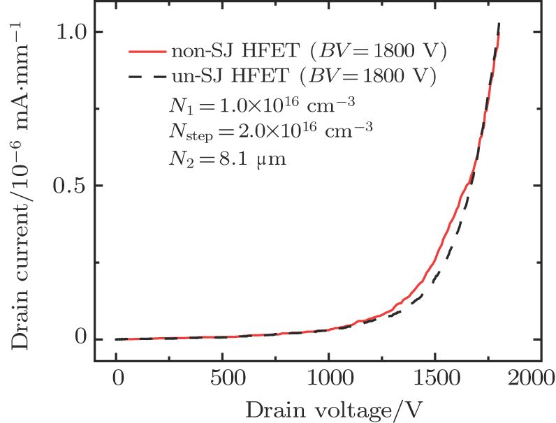
 | Fig. 2. (color online) On-state I–V characteristics for two devices, showing (a) transfer characteristics, (b) output characteristics. |
 | Fig. 3. (color online) Off-state I–V characteristics corresponding to the devices in Fig. |
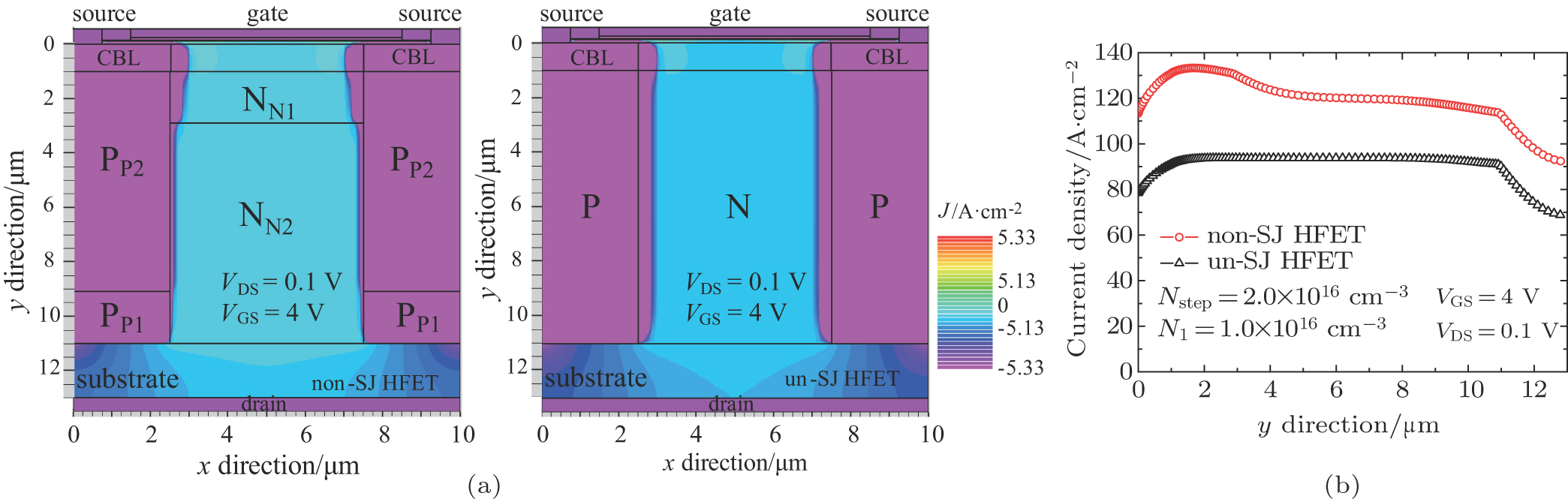
A physical insight into the improvement in non-SJ HFET could be achieved according to on-state current density distributions as well as off-state equipotential lines and electric field distributions. At on-state for both devices in Fig. 


 | Fig. 4. (color online) On-state current density distributions corresponding to the devices in Fig. |
The breakdown performances in non-SJ HFET and un-SJ HFET are illustrated in Fig.
 | Fig. 5. (color online) Off-state performances in two devices at breakdown voltage corresponding to Fig. |
4. Optimization and design for minimized RonA without deterioration in BV
Figure 


 | Fig. 6. (color online) Plots of breakdown voltage and specific on-resistance versus H2 at different values of 

|
 | Fig. 7. (color online) Vertical electric field distributions along the line A1A2 in corresponding non-SJ HFETs with different values of H2 in Fig. |
Figure 


 | Fig. 8. (color online) Plots of breakdown voltage and specific on-resistance versus H2 at different values of 

|
 | Fig. 9. (color online) BV and reductions in RonA for optimized results at different values of N1 and 
|
N1, the reduction in RonA could be improved by increasing 


5. Fabrication process
Nowadays, thick in situ doping GaN layer growth technologies,[22,23] GaN-based selective area growth technologies (SAG),[14,24] and GaN etching technologies have become more and more mature.[25,26] The reported highest GaN pillar height by SAG and the deepest etching trench by plasma etching technology have been more than 
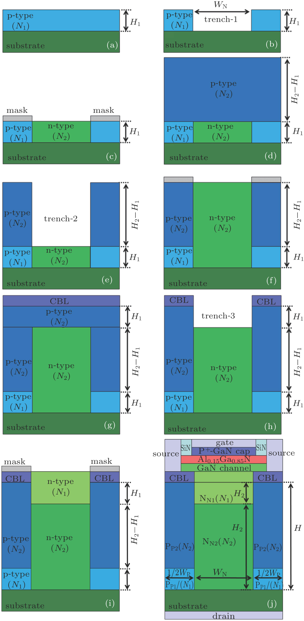
As an example, the following gives a feasible process approach of the proposed non-SJ HFET based on the methods mentioned in Refs. [14] and [24], as illustrated in Fig. 


 | Fig. 10. (color online) A feasible process approach of the proposed non-SJ HFET, showing (a) (N1 doping and H1 thickness) p-type GaN layer growth, (b) trench-1 etching, (c) n-type GaN layer regrowth in trench-1, (d) (N2 doping and H2–H1 thickness) p-type GaN layer growth, (e) trench-2 etching, (f) n-type GaN layer regrowth in trench-2, (g) (N2 doping and H1 thickness) ptype GaN layer and CBL growth, (h) trench-3 etching, (i) n-type GaN layer regrowth in trench-3, and (j) completed device. |
6. Conclusions
In this paper, a novel non-SJ HFET based on the nonuniform doping superjunctions (non-SJs) is presented by two-dimensional simulations, with emphasis on the minimized RonA at no expense of BV. Systematical studies and analyses of the device on- and off-state performance, device physical mechanisms as well as device optimization designs are conducted. The simulation results exhibit that the remarkable reduction in RonA with the same BV as that of un-SJ HFET, could be realized by modulating the doping concentration and thickness of the light and heavy doping parts in non-SJ. These results demonstrate the potential and advantage of non-SJ HFET in high power electronic applications.
Reference
| [1] | |
| [2] | |
| [3] | |
| [4] | |
| [5] | |
| [6] | |
| [7] | |
| [8] | |
| [9] | |
| [10] | |
| [11] | |
| [12] | |
| [13] | |
| [14] | |
| [15] | |
| [16] | |
| [17] | |
| [18] | |
| [19] | |
| [20] | |
| [21] | |
| [22] | |
| [23] | |
| [24] | |
| [25] | |
| [26] | |
| [27] | |
| [28] |