Low specific on-resistance GaN-based vertical heterostructure field effect transistors with nonuniform doping superjunctions
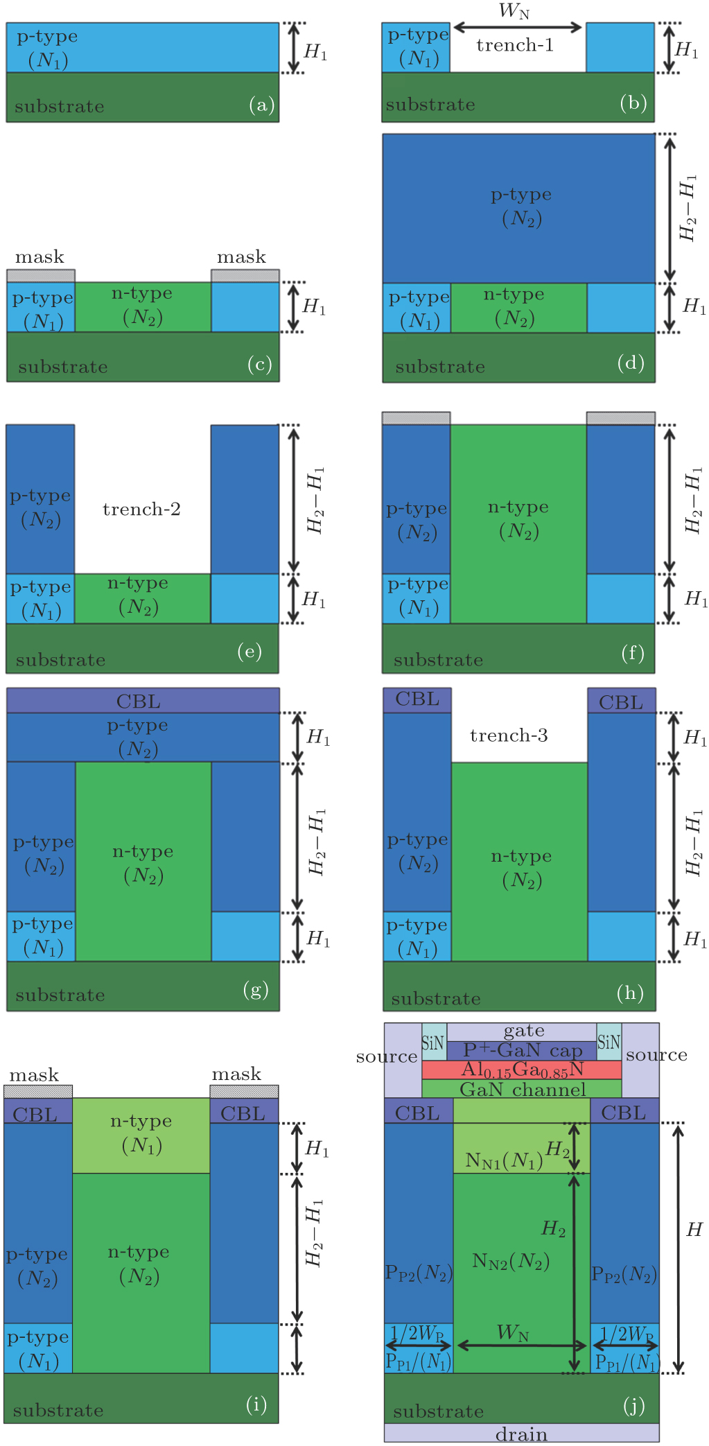
(color online) A feasible process approach of the proposed non-SJ HFET, showing (a) (

Low specific on-resistance GaN-based vertical heterostructure field effect transistors with nonuniform doping superjunctions |
|
(color online) A feasible process approach of the proposed non-SJ HFET, showing (a) ( |
 |