Magnesium incorporation efficiencies in MgxZn1−xO films on ZnO substrates grown by metalorganic chemical vapor deposition
Hu Qi-Chang1, Kai Ding2, †
College of Mechanical and Electronic Engineering, Fujian Agriculture and Forestry University, Fuzhou 350002, China
Key Laboratory of Optoelectronic Materials Chemistry and Physics, Fujian Institute of Research on the Structure of Matter, Chinese Academy of Sciences, Fuzhou 350002, China


† Corresponding author. E-mail: kding@fjirsm.ac.cn

Abstract

We investigate the magnesium (Mg) incorporation efficiencies in MgxZn1−xO films on c-plane Zn-face ZnO substrates by using metalorganic chemical vapor deposition (MOCVD) technique. In order to deposit high quality MgxZn1−xO films, atomically smooth epi-ready surfaces of the hydrothermal grown ZnO substrates are achieved by thermal annealing in O2 atmosphere and characterized by atomic force microscope (AFM). The AFM, scanning electron microscope (SEM), and x-ray diffraction (XRD) studies demonstrate that the MgxZn1−xO films each have flat surface and hexagonal wurtzite structure without phase segregation at up to Mg content of 34.4%. The effects of the growth parameters including substrate temperature, reactor pressure and VI/II ratio on Mg content in the films are investigated by XRD analysis based on Vegard’s law, and confirmed by photo-luminescence spectra and x-ray photoelectron spectroscopy as well. It is indicated that high substrate temperature, low reactor pressure, and high VI/II ratio are good for obtaining high Mg content.

1. Introduction

ZnO and its base ternary alloys are promising candidates for optoelectronic applications in the ultraviolet region, owing to their direct wide bandgaps and large exciton binding energies. By incorporating magnesium (Mg) into the ZnO matrix, the energy bandgaps of MgxZn1−xO alloys can be adjusted from 3.3 eV to 7.8 eV.[1] Hence MgxZn1−xO alloy is considered as a suitable material for energy engineering in ZnO-based low-dimensional optoelectronic devices. There have been numerous reports on MgxZn1−xO/ZnO heterostructure devices, including single heterostructure ultraviolet light-emitting diodes[2] metal–semiconductor–metal solar-blind photodetectors,[3] field-effect transistors,[4] etc.

However, the growth of MgxZn1−xO is complicated for the different stable structures of ZnO (wurtzite) and MgO (rocksalt). Poor crystalline quality and phase separation are thus problems that have to be resolved.[5] Besides, large lattice-mismatch between the commonly used substrates and films and low Mg incorporation efficiency in the MgxZn1−xO films are also important factors responsible for deteriorating the crystalline quality. According to the phase diagrams of ZnO–MgO binary systems, the thermodynamic solid solubility of MgO in a ZnO matrix is normally less than 4%.[5] Nevertheless, previous studies have shown that single wurtzite structure MgxZn1−xO films can be acquired with significant Mg compositions up to 33%∼49%.[1,6,7] The large variation of incorporation efficiency in MgxZn1−xO alloys might be attributed to the non-thermal equivalent natures of different techniques and growth conditions. Therefore, it is necessary to understand the effects of the growth parameters on Mg incorporation efficiency in MgxZn1−xO thin films.

Several methods have been employed to grow MgxZn1−xO alloys, including pulsed laser deposition (PLD),[8] magnetron sputtering,[3,9] molecular beam epitaxy (MBE),[4,10] and metalorganic chemical vapor deposition (MOCVD).[11,12] Among these methods, MOCVD is a promising technique for industrial applications due to its advantages of high growth rate, large-area deposition, and good thickness and composition uniformity.

It is reasonable that closely lattice-matched substrates are favorable for the epitaxial growth of the films. Therefore, the quality of wurtzite structure MgxZn1−xO films can be improved by using ZnO single crystal as substrate without a buffer layer, owing to their naturally matched lattice. The MgxZn1 −xO is crucial for serving as a barrier layer or quantum wells in ZnO/MgxZn1−xO heterostructures, and high quality of MgxZn1−xO films would promote the performance of the device.[2] High quality MgxZn1−xO films grown on ZnO single crystal also were proved to be important for fabricating superior solar-blind photodetectors.[3] Although ZnO single crystal substrates are already commercially available and some research has been dedicated to the homoexpitaxial growth of ZnO films on them,[13] the systematical study of MgxZn1−xO film growth on ZnO substrates is very important but still lacking. This can be attributed to various factors, such as high cost-level of device-grade ZnO substrates, immature surface treatment technique, and highly variable quality of crystal structure. We have reported the hydrothermal growth of ZnO single crystals with new mineralizers and low-cost liners. A large-sized ZnO single crystal whose x-ray θ–rocking curve has a full width at half maximum (FWHM) of 36 arcsec for (002) reflection and a room temperature electron mobility of 239 cm2/V·s has been obtained.[14] In this study, we report on the epitaxial growth of MgxZn1−xO films on Zn-face of ZnO substrates by MOCVD. Growth parameter dependence of the Mg incorporation efficiency in the films is systematically discussed.

2. Experiments

The MgxZn1−xO thin films investigated in this study were deposited by a vertical and resistively heated MOCVD on c-plane ZnO substrates grown by the hydrothermal method. The ZnO substrates were 10 mm×10 mm×0.5 mm in size. Before being sent to the reactor, they were chemo-mechanically polished followed by thermal annealing in O2 atmosphere. For the preparation details as well as structural and optical properties of the ZnO substrates, the readers can refer to Ref. [14]. Biscyclopentadienyl-magnesium (Cp2Mg), diethyl-zinc (DEZn) and oxygen (O2, 7N) were used as the precursors for Mg, Zn, and O, respectively. Ultra-high purity N2 (9N) was used as the carrier gas. In order to prevent the gas phase reactions, O2 and metal–organic sources were introduced separately into the reactor and just mixed below the susceptor. The flow rates of Cp2Mg and DEZn were fixed at 2800 sccm and 25 sccm respectively, resulting in a Cp2Mg/DEZn ratio of 2:1. The O2 flow rate was varied between 60 sccm and 200 sccm to regulate the VI/II ratio (the molar flow ratio of O2/(Cp2Mg+DEZn)). Process pressure in the reactor was varied from 10 Torr to 250 Torr (1 Torr = 1.33322×10² Pa). The substrate temperature ranged from 380 °C to 460 °C. The susceptor rotating speed was 1000 rpm. All the films were deposited for one hour.

The surface morphologies of ZnO substrates and MgxZn1−xO films were investigated using atomic force microscope (AFM) and scanning electron microscope (SEM). The structure properties of MgxZn1−xO films were analyzed by x-ray diffraction (XRD) in θ–2θ geometry using PANalytical X’ Pert PRO with Cu Kα source. The Vegard’s law has been verified to be a good model for MgxZn1−xO alloys due to the similar size of Zn ion (0.60 Å) to that of Mg ion (0.57 Å).[6,1517] Mg content in MgxZn1−xO films was determined by the calculation of c-axis lattice parameter following the Vegard’s law. Photo-luminescence (PL) spectra were obtained at room temperature by using a He–Cd laser (325 nm) as the excitation light source. X-ray photoelectron spectroscopy (XPS) was also applied to MgxZn1−xO films to study the change of Mg content.

3. Results and discussion

It has been shown that the surface of ZnO substrate plays a crucial role in the quality of the epitaxial growth of thin film.[18] Various treatment methods for ZnO substrates including thermal annealing, wet-chemical etching and plasma treatment have been proposed to obtain an atomically flat surface.[1921] In this study, thermal annealing technique is employed for chemo-mechanically polished ZnO substrates. Many uniformly sized islands on a smooth surface can be seen in the AFM image of as-polished ZnO substrate (Fig. 1(a)), which is considered as a result of the damage induced by the sawing and polishing technique. After annealing the ZnO substrate at 1100 °C in O2 atmosphere for 30 min, the islands disappear and the terrace-like structure can be observed. It indicates that the thermal annealing treatment can eliminate surface damage and lead to a significant improvement of the surface quality (Fig. 1(b)). Typical step height is 2 nm equivalent to 4 unit cells (lattice parameter c ∼ 0.52 nm). Figure 1(c) shows the surface of a MgxZn1−xO film with Mg content of about 30% grown on the annealed ZnO substrate, presenting an RMS roughness of 2.236 nm.

Fig. 1. (color online) Atomic force microscopy images of (a) the as-polished and (b) as-annealed ZnO substrate, and (c) MgxZn1−xO film grown on the annealed ZnO substrate.

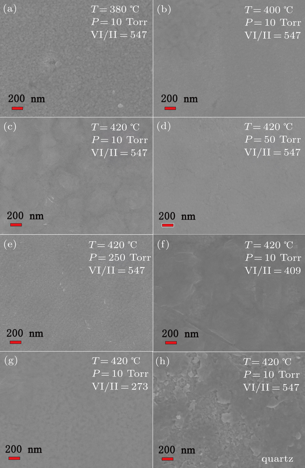
The SEM images of MgxZn1−xO films grown on ZnO substrates at various growth parameters are shown in Figs. 2(a)2(g). As can be seen in Figs. 2(a)2(g), the surface morphologies of MgxZn1−xO films on ZnO substrates are mainly smooth in a range of growth parameters. If observed carefully, it will be found that some pores exist on the surface at low growth temperature, and the surface is smoother with the increase of growth temperature (shown in Figs. 2(a) and 2(c)). This can be attributed to an improvement of the crystalline quality of the films with increasing temperature, which is verified from the following XRD analyzing results. For comparison, an image of MgxZn1 −xO film grown on quartz substrate is also included in Fig. 2(h). Rough surface, poor quality film is obtained on the quartz substrate at the same growth parameters (shown in Figs. 2(c) and 2(h)). The above results demonstrate that the ZnO substrate annealed at 1100 °C in O2 atmosphere for 30 min is appropriate for epitaxial growth and the MgxZn1−xO thin films investigated in this study have smooth morphologies.

Fig. 2. (color online) Scanning electron microscope images of MgxZn1−xO films grown on ZnO substrate at various growth parameters: ((a), (b), and (c)) various growth temperatures; ((c), (d), and (e)) various reactor pressure; ((c), (f), and (g)) various VI/II ratios; (h) MgxZn1−xO films grown on quartz substrate as a reference.

The effects of growth parameters on the incorporation of Mg component are discussed below. We first investigate Mg incorporation efficiencies in MgxZn1−xO films at various growth temperatures (from 380 °C to 460 °C), while the reactor pressure and the VI/II ratio are kept at 10 Torr and 545, respectively. XRD patterns of the samples are shown in Fig. 3(a). The enlarged image of specific angle range is seen in Fig. 3(a). At a relatively low temperature of 380 °C, only (002) and (004) peaks of ZnO substrate can be seen. The split between Kα1 and Kα2 diffraction lines reveals a high quality of the substrate. However, Kα2 line may overlap (002) peak from MgxZn1 −xO film with low Mg content, which affects the determination of Mg content. When the temperature increases to 400 °C, (002) peak of MgxZn1−xO film begins to arise. As the substrate temperature further increases, MgxZn1−xO diffraction peak shifts toward a higher diffraction angle with the increase of its intensity than (002) ZnO peak. The angle shift must originate from the increase of Mg content in the film due to the linear decrease of the c-axis lattice constant of the film with the increase of the Mg content. On the other hand, the increase of the peak intensity indicates an improvement of the crystalline quality of the films with increasing substrate temperature.

Fig. 3. (color online) (a) Patterns of x-ray diffraction 2θθ scan for different substrate temperatures; (b) the enlarged image of specific angle range; (c) dependence of Mg composition (%) on substrate temperature.

Since the film is thick enough and exceeds its critical thickness value, the strain in the film is assumed to be completely relaxed. Following Vegard’s law, we determine Mg content according to the relationship c = 5.2029 − 0.0020 x that is deduced from Fig. 3(b) in Ref. [15]. The calculated results (2θ, c-lattice constant, and Mg content) are summed up in Table 1. Figure 3(c) exhibits the dependence of Mg content on substrate temperature. It can be seen that only relatively low Mg content (below 35%) can be acquired at a high Cp2Mg/DEZn ratio of 2:1. The low incorporation efficiency of Mg atom into MgxZn1−xO is mainly caused by the low decomposition rate of Cp2Mg. The semi-decomposition temperature of DEZn is 280 °C, and complete-decomposition temperature is 360 °C.[22] When the substrate temperature exceeds 380 °C, DEZn is completely decomposed. While Cp2Mg has higher decomposition temperature, and the decomposition rate of Cp2Mg increases as temperature increases. Therefore, higher temperature contributes to higher Mg incorporated efficiency. No peaks belonging to the (111) direction of MgO are detected in Fig. 3(a), indicating the absence of phase separation in the films. This may be partly ascribed to the adoption of high-quality ZnO substrate.

Table 1.

Calculated results of the effect of the substrate temperature.

.

Figures 4(a) and 4(b) display XRD patterns of MgxZn1−xO films grown under different reactor pressures, while substrate temperature and VI/II ratio are fixed at 420 °C and 545 respectively. Under 10 Torr, both (002) diffraction peaks of ZnO substrate and MgxZn1−xO film appear. The 2θ angle of MgxZn1−xO film at 34.86° indicates Mg content of 30.84%, and it decreases to 34.80° when grown under 50 Torr, which means that the Mg content decreases down to 26.55%. When the reactor pressure further increases to 250 Torr, the peak corresponding to (002) plane of MgxZn1−xO film becomes undetectable, suggesting that Mg content in the film is very low. The calculated results, presented in Fig. 4(c) and Table 2, indicate that low reactor pressure will enhance Mg incorporation efficiency in the film. The raising of the reactor pressure will reduce the thickness of the boundary layer above the substrate atmosphere, and enhance the parasitic reactions. Excessive parasitic reactions in the reactor will suppress the diffusion ability of Mg atoms. Consequently, Mg incorporation efficiency is reduced.

Fig. 4. (color online) Patterns of (a) x-ray diffraction 2θθ scan for different reactor pressures; (b) the enlarged patterns of specific angle range; (c) the relationships of the Mg composition (%) with reactor pressure.
Table 2.

Calculated results of the effect of the reactor pressure.

.

As shown in Figs. 5(a) and 5(b), MgxZn1 −xO thin films are grown at various VI/II ratios (273, 409, and 545), while substrate temperature and reactor pressure are fixed at 420 °C and 10 Torr, respectively. With the increase of VI/II ratio, MgxZn1−xO diffraction peak shifts toward higher diffraction angle from 34.82 to 34.86, corresponding to Mg content increasing from 27.98% to 30.84%. The assessed values of Mg content in MgxZn1−xO films are shown in Table 3. Accordingly, the dependence of the Mg content in the film on VI/II ratio is presented in Fig. 5(c). Such a monotonic increase of Mg content with increasing VI/II ratio may be attributed to the suppression of the gas phase nucleation. When the film is grown under high VI/II ratio, the partial pressure of Mg in the gas phase relatively declines, and then the nucleation of Mg in the gas phase is suppressed. It leads to more Mg atoms diffusing on the substrate, which may cause the Mg atoms to be substituted for Zn sites. Thus, Mg incorporated efficiency in the MgxZn1−xO film is promoted.

Fig. 5. (color online) Patterns of (a) x-ray diffraction 2θθ scan for different VI/II ratios; (b) the enlarged patterns of specific angle range; (c) dependence of the Mg composition (%) on VI/II ratio.
Table 3.

Calculated results of the effect of the VI/II ratio.

.

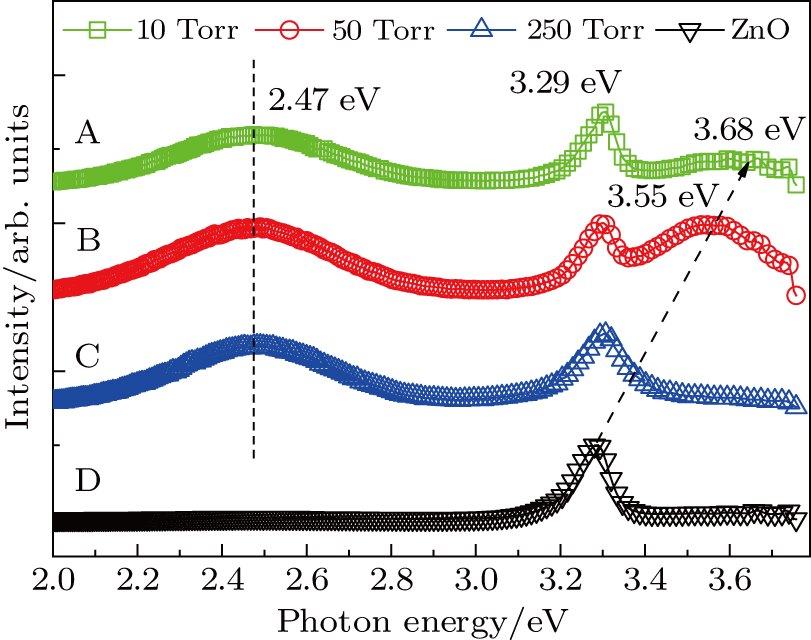
To further verify the above results, PL and XPS measurements are performed on the samples under different reactor pressures. Figure 6 displays the PL spectra of MgxZn1−xO films under different reactor pressures (see Figs. 6(a)6(c)), which are measured at room temperature. For comparison, the PL spectra of ZnO film grown on ZnO substrate are also included in Fig. 6 (see Fig. 6(d)). All samples show near-band-edge (NBE) emissions centered at 3.29 eV due to free excitonic emission of ZnO single crystal substrate.[23] When the signal of film is weak or close to the substrate signal, it will be easily affected by the strong signal at the band edge from ZnO single crystal. This is the reason that only the peak at 3.29 eV can be observed in samples D (x = 0) and C (low Mg content at 250 Torr). However, the band-gap energy of MgxZn1−xO film depends on Mg content, which results in a blueshift of the NBE emission peak as indicated by the dotted line (from 3.29 eV to 3.68 eV). Besides, the general consensus is that a visible defect-band peaked at 2.47 eV, is mainly due to oxygen vacancy (Vo) native defects in the film.[24,25] This behavior of the PL spectrum is in good agreement with that of the XRD analysis result.

Fig. 6. (color online) PL spectra of MgxZn1−xO films under different reactor pressures.

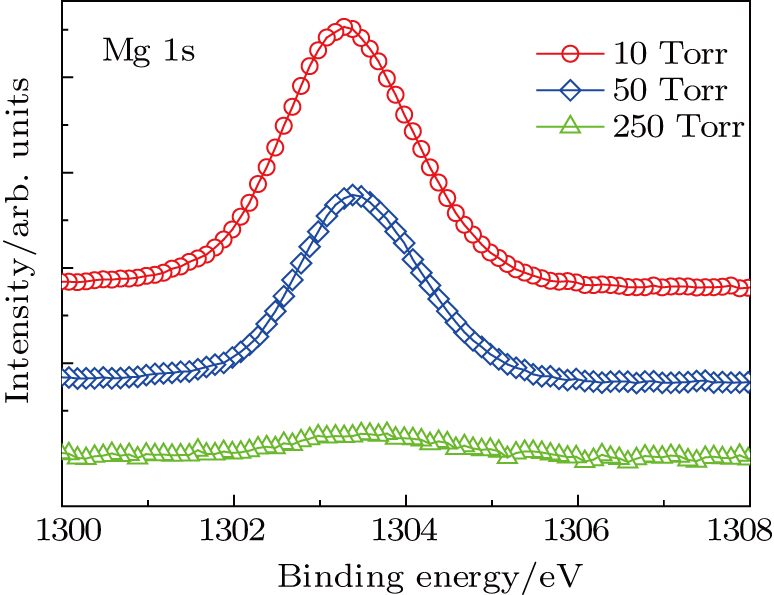
Figure 7 shows the core-level lines of Mg 1s of the MgxZn1−xO film under reactor pressures of 10 Torr, 50 Torr, and 250 Torr, respectively (recorded after 20-s Ar sputtering). As reactor pressure increases, the Mg 1s peak intensity decreases. The Mg content values in the MgxZn1 −xO films are determined to be 33.8%, 26.3%, and 5.6%, respectively. This is direct evidence for the fact that Mg content decreases with the increase of reactor pressure. The trend of XPS spectrum results is in good agreement with the variation trends of PL and XRD analysis result.

Fig. 7. (color online) XPS spectra of Mg 1s of MgxZn1−xO films under different reactor pressures, recorded after 20-s Ar sputtering.
4. Conclusions

In this work, single hexagonal phase MgxZn1−xO films with various values of Mg content are synthesized by MOCVD on c-plane Zn-face ZnO substrates. AFM images and SEM images demonstrate that MgxZn1−xO films each with flat surface can be obtained on appropriately thermally treated substrates. Systematical XRD, PL, XPS analyses reveal that high substrate temperature, low reactor pressure, and high VI/II ratio are needed to enhance the Mg incorporation efficiency in MgxZn1−xO films.

Reference
[1] Yang W Vispute R D Choopun S Sharma R P Venkatesan T Shen H 2001 Appl. Phys. Lett. 78 2787
[2] Nakahara K Akasaka S Yuji H Tamura K Fujii T Nishimoto Y Takamizu D Sasaki A Tanabe T Takasu H Amaike H Onuma T Chichibu S F Tsukazaki A Ohtomo A Kawasaki M 2010 Appl. Phys. Lett. 97 013501
[3] Zheng Q H Huang F Ding K Huang J Chen D G Zhan Z B Lin Z 2011 Appl. Phys. Lett. 98 221112
[4] Sasa S Maitani T Furuya Y Amano T Koike K Yano M Inoue M 2011 Phys. Status Solidi 208 449
[5] Sarver J F Katnack F L Hummel F A 1959 J. Electrochem. Soc. 106 960
[6] Ohtomo A Kawasaki M Koida T Masubuchi K Koinuma H Sakurai Y Yoshida Y Yasuda T Segawa Y 1998 Appl. Phys. Lett. 72 2466
[7] Park W I Yi G C Jang H M 2001 Appl. Phys. Lett. 79 2022
[8] Ryoken H Ohashi N Sakaguchi I Adachi Y Hishita S Haneda H 2006 J. Cryst. Growth 287 134
[9] Kim I S Lee B T 2009 J. Cryst. Growth 311 3618
[10] Li D H Wang H Q Zhou H Li Y P Huang Z Zheng J C Wang J O Qian H J Ibrahim K Chen X Zhan H Zhou Y Kang J 2016 Chin. Phys. 25 076105
[11] Liu K Pierce J M Ali Y S Krahnert A Adekore B T 2011 J. Appl. Phys. 109 083524
[12] Fan H B Zheng X L Wu S C Liu Z G Yao H B 2012 Chin. Phys. 21 038101
[13] Muret P Tainoff D Morhain C Chauveau J M 2012 Appl. Phys. Lett. 101 122104
[14] Lin W W Chen D G Zhang J Y Lin Z Huang J K Li W Wang Y H Huang F 2009 Cryst. Growth Des. 9 4378
[15] Sadofev S Blumstengel S Cui J Puls J Rogaschewski S Schafer P Sadofyev Y G Henneberger F 2005 Appl. Phys. Lett. 87 091903
[16] Zhang T C Venkatachalapathy V Azarov A Y Trunk M Galeckas A Kuznetsov A Y 2011 J. Cryst. Growth 333 66
[17] Pan C J Hsu H C Cheng H M Wu C Y Hsieh W F 2007 J. Solid State Chem. 180 1188
[18] Ogata K Kawanishi T Sakurai K Kim S W Maejima K Fujita S Fujita S 2002 Phys. Status Solidi 229 915
[19] Graubner S Neumann C Volbers N Meyer B K Blasing J Krost A 2007 Appl. Phys. Lett. 90 042103
[20] Nakamura T Masuko K Ashida A Yoshimura T Fujimura N 2011 J. Cryst. Growth 318 516
[21] Dong Y F Fang Z Q Look D C Doutt D R Cantwell G Zhang J Song J J Brillson L J 2010 J. Appl. Phys. 108 103718
[22] Sallet V Thiandoume C Rommeluere J F Lusson A Riviere A Riviere J P Gorochov O Triboulet R Munoz-Sanjose V 2002 Mater. Lett. 53 126
[23] Bao S Y Dong W J Xu X Luan T B Li J Zhang Q Y 2011 Acta Phys. Sin. 60 036804 in Chinese
[24] Yu X X Zheng H M Fang X Y Jin H B Cao M S 2014 Chin. Phys. Lett. 31 117301
[25] Ning S Zhan P Xie Q Wang W Zhang Z 2015 J. Mater. Sci. Technol. 31 969