† Corresponding author. E-mail:
Project supported by the National Natural Science Foundation of China (Grant No. 61377061), the Public Project of Zhejiang Province, China (Grant No. 2014C31146), and sponsored by K. C. Wong Magna Fund in Ningbo University, China.
Chalcogenide glasses have shown promise in fabricating mid infrared (MIR) photonic sensing devices due to their excellent optical properties in MIR. In addition, the glass transition temperature of chalcogenide glasses are generally low, making them ideal to create the high-throughput patterns of micro-scale structures based on hot embossing that is alternative to the standard lithographic technology. In this paper, we outline the research progress in the chalcogenide waveguide based on the hot embossing method, and discuss the problems remaining to be solved and the possible solutions.
Molecular species exhibit specific vibrational absorption bands in the mid-infrared (MIR) region spanning a wavelength range from 3 µm to 25 µm.[1] Tsay et al.[2] indicated that MIR sensors, which are based on evanescent field sensing of molecular species, can detect the molecules at very low concentrations by using their absorption fingerprints with high sensitivity and selectivity over a wide range of compounds without labeling, and thus are potential to be applied to low-cost, widely-accessible health and environmental monitoring.[3] To detect these molecules, it is essential to develop waveguides and integrated optical devices for evanescent field based sensing in the MIR. Widely used silicate glasses do not transmit at the wavelengths beyond 3 µm, while the fluoride glasses degrade when they are in contact with water. These conventional materials that are well-characterized for the applications in the telecommunications wavelengths are not suitable for the applications in MIR. In contrast, chalcogenide glasses (ChGs), consisting of one or more chalcogen elements such as S, Se, and Te, together with other elements such as Ge, Ga, As, Si, P, and Sb,[4] are transparent in a wide range from 1 µm to 25 µm, depending on the chemical compositions,[5] covering the widely used atmospheric IR windows of 3 µm–5 µm and 8 µm–14 µm. Moreover, chalcogenide glasses are generally inert against moisture and harsh chemical surroundings, and thus are potential to be used for creating integrated devices for MIR sensing and defense applications.[6,7]
The development of chalcogenide waveguide firstly dated back to the early 1970s. Bessonov et al.[8] reported a chalcogenide waveguide fabricated in the form of a thin As–Se chalcogenide glass film on a barium fluoride single-crystal substrate and the attenuation coefficient measured to be 3 dB/cm for the dominant TE mode. With the further development of the fabrication techniques, Viens et al.[9] reported amorphous multilayer As24S38Se38/As2S3 thin film deposited on a silicon wafer by conventional thermal evaporation and photolithography followed by chemical wet etching. Although waveguide optical loss was found to be 1 dB/cm at 1300 nm, chalcogenide waveguide structure was damaged partially (the glass sidewall etching produced ridges with a trench angle of about 45°) because most chalcogenide materials can be dissolved in alkaline resist developer NH4OH.[10] Since the wet etching method is not easy to control, and the waveguides produced always contain particle contamination and are lack of anisotropy, more recently, plasma dry etching together with photolithography technique are usually employed to fabricate the optical waveguide. Hu et al.[11] reported the fabrication of the planar waveguides from thermally evaporated Ge23Sb7S70 films by using plasma etching, the waveguide exhibits a sidewall root mean square (RMS) roughness of 17 nm–20 nm, and an optical propagation loss of 3 dB/cm–5 dB/cm at 1550 nm. To obtain better etching results, the advanced technologies like ion etching, inductively coupled plasma (ICP) technology and electron cyclotron resonance technology, have been used to fabricate chalcogenide optical waveguides. Ruan et al.[12] reported the fabrication of the low loss As2S3 rib waveguides made by standard photolithography technique combined with ICP, and the minimum propagation loss of the waveguide is 0.25 dB/cm at 1550 nm. Madden et al.[13] demonstrated that the As2S3 waveguides with lengths up to 22.5 cm reduce the losses down to 0.05 dB/cm at 1550 nm, which is the lowest ever reported etched by ICP.
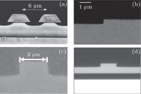 | Fig. 1. (a) SEM micrograph of a multilayer As24S38Se38/As2S3 rid waveguide processed by lithography and wet etching (Viens et al.).[9] (b) Cross-sectional image of Ge23Sb7S70 waveguide patterned by SF6 plasma etching (Hu et al.).[11] (c) SEM micrograph showing the profile of As2S3 waveguide etched by ICP and coated with polysiloxane cladding (Ruan et al.).[12] (d) Optical micrograph of cleaved finished waveguide in the 2.6-µm thick As2S3 film (Madden et al.).[13] |
However, it is not easy to use standard photolithography followed by dry plasma etching to fabricate waveguides with high-efficiency because chalcogenides are susceptible to attack by the alkaline-based chemicals used in photolithography as well as by most gases in plasma etching. Thus some additional steps are needed, thereby leading to more complexities and less control than ideal process. All these relevant facilities require large capital investment and are not ideal for commercial large-scale production.
Hot embossing, also known as nano-imprinting, initially proposed and developed for polymeric materials by Chou et al.,[14,15] is an emerging lithographic technology that is based on surface patterning. It requires only a single step to fabricate complicated optical device and produce even nanometer sized features without using the chemical processing.[15–18] In contrast to standard photolithography technology, the hot embossing is extremely fast, simple and low cost, which makes it promise in large-scale production. Hot embossing is in line with the development direction of “easy” and “miniaturization” of the optoelectronic device preparation technology, hence it has received more and more attention of some well-known research institutions in recent years. In this paper, we review the fabrication of chalcogenide rib waveguide with using hot embossing and discuss further development and potential applications of this approach.
Several groups have demonstrated the possibility of molding chalcogenide glasses against a stamp to make rib waveguides.[19–25] The process of hot-embossing is conceptually straightforward: chalcogenide film (deposited on silicon wafer) is heated to a temperature above its Tg (glass transition temperature), pressed against a stamp isothermally for a certain time under a prescribed load. After the removal of the load, chalcogenide film sample is cooled to ambient temperature, and then separated from the stamp manually due to tremendous differences in thermal expansion coefficient between the film and stamp material. The stamp imprint is retained in the film surface and then the desired waveguide structure is fabricated. The replication accuracy mainly depends on the quality of the surface finish of the stamp and thus it is repeatable to fabricate successive waveguides with the same stamp.[26] There are two main stamps used for hot-embossing: hard stamp and soft stamp. Hard stamp which consists of metal (e.g. Ni), silicon, fused silicon, silicon-on-insulator or metal-coated hard polymers, is usually made by e-beam lithography and wet-etching and imprinted on small areas at high loads.[27] On the other hand, soft stamp can realize multiple and diverse uniform patterning and is more tolerant to the tilt between the stamp and sample than hard stamp.[28] In addition, soft stamp is easily obtained by casting on a single master mould over large areas with excellent accuracy and reproducibility. Currently, polydimethylsiloxane (PDMS) stamp is widely used because it is sufficiently durable to permit many pattern replications and allows the production of the waveguides with no stamp release issues and good uniformity.[24,27]
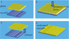 | Fig. 2. (color online) Schematic flow chart of the hot embossing process. (Seddon et al. 2014).[26] |
ChGs are metastable and long-range disordered materials, and compared with the crystalline material, their bonded or atomic structures tend to be more prone to change when exposed to illumination with light, thermal treatment, electromagnetic radiation and particle beam bombardment.[29] That is because (i) chalcogenide glass has a lower spatial mean coordination number (MCN), which means that it has a high degree of freedom and structural flexibility and (ii) chalcogen atoms are two-coordinated and have two high-lying lone-pair electrons on the top of its valence bands. When the chalcogenide glass is exposed to laser light, these nonbonding lone-pair electrons are readily excited across the bandgap by the absorption of light, leading to changes in physical and optical properties of chalcogenide glass. Some distinct photoinduced phenomena are observed in amorphous chalcogenides, including photocrystallization, photovaporization, photodecomposition, photocontraction or expansion, photodarkening or photobleaching, etc. These changes are accompanied by changes in the electronic band gap, refractive index and optical absorption coefficient.[4] To summarize, ChGs exhibit distinct photosensitivity and devices such as gratings and waveguides can be fabricated in ChGs by using their photoinduced effects.[30–33] However, the excellent photosensitivity of ChGs is undesirable for fabricating waveguides via hot-embossing. Therefore, it is essential that the core material in the rib waveguide should have good photo stability and high thermal stability (i.e., it remains amorphous and does not devitrify, crystallize in the hot embossing process). Most of selenide-based glass materials have been chosen as the core glasses for fabricating waveguides via hot-embossing due to their excellent glass stability during manufacture under ambient conditions.[21–24] Generally, the waveguide is based on the chalcogenide film on an oxidized silicon wafer. For evanescent-field-mediated sensing, some groups have also employed a bulk chalcogenide glass with a lower refractive index as both the substrate and optical under-cladding (chalcogenide-on-chalcogenide).[21,22,24] To select the core and cladding glasses to make a high numerical aperture (NA) single-mode waveguide, some criteria should be meet: i) thermal expansion coefficient mismatching between the core and cladding glasses should be minimum; and ii) the cladding glass should have a higher Tg than the core glass, and this enables a range of temperatures in which the substrate is either solid or much viscous compared with the supercooled liquid thin film in this temperature range.
Several methods have been used to deposit high quality chalcogenide film, including thermal evaporation, radio-frequency (RF)-magnetron sputtering, ultra-fast laser ablation and collosol-gelling method. Each method has its own advantages and drawbacks, and currently thermal evaporation and radio-frequency (RF) sputtering are two main methods to deposit the films. During the thermal evaporation, the source material to be evaporated is placed in a boat and connected to a power supply for heating under vacuum conditions. When heated to a certain temperature, the solid source material is converted into gaseous particles with certain kinetic energy, leaping into high-vacuum space, and finally deposited onto the substrate surface. Thermal evaporation is convenient to prepare large-area thick film with a relatively high deposition speed, but it has problems that the deviation of component between source material and deposited film is relatively large if I) depositing materials have high melting points and II) multi-components and/or composite materials have a large melting point difference between their constituents.[34] Because non-congruent evaporation occurs, the evaporated particles with high saturated vapor pressure tend to deposit on the substrate preferentially, resulting in nonhomogeneous films. Zakery and Elliot argued that thermal evaporation might not be suitable for the accurate transfer of the stoichiometry of the multicomponent glass films.[35] Besides, the reproducibility of the film composition is not ensured and the film thickness is difficult to control precisely. On the other hand, RF sputtering is usually performed in an Argon (Ar) gas atmosphere in an evacuated chamber. When the target surface is bombarded with generated Ar+ ions, the solid atoms emitted from the sputtered material are condensed and deposited on the surface of the substrate. Unlike thermal evaporation, RF sputtering can ensure the exact reproducibility of the film composition. However, the deposition-rate of RF-sputtering is low and the column-like structures always can be found in the deposited films, resulting in porosity.[36,37] Balan et al.[37] demonstrated the refractive indexes of these films were shown to decrease with increasing film thickness because of a change in the morphology (porosity) of the film.
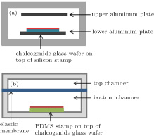
There are two different approaches to hot-emboss the waveguide device: hard and soft-pressing. In the former case, the pressing facility consists of a vacuum chamber and two flat and parallel aluminum plates. The upper aluminum plate is fixed and the lower one can be raised with applied force. After the stamp is placed on the lower plate where the patterned face is up, the sample is placed on the top of the stamp where the sputtered film is faced down to the patterned stamp surface, both aluminium plates are heated to a certain temperature, and then the lower aluminium plate will be raised to accomplish the embossing [see Fig.
Pan et al. (2008)[21] reported a chalcogenide-glass mono-mode rib waveguide fabricated by hot-embossing through using a hard silicon stamp first in a one-step ‘fiber-on-glass’ approach involving two types of chalcogenide glasses (core/under-clad: As40Se60/Ge17As18Se65). The As40Se60 fibers were hot-pressed between a silicon stamp (the fibers are aligned such that each fiber lay in one channel in the stamp) and a polished and flattened Ge17As18Se65 glass substrate. One of the waveguides was an As–Se rib core with a width of 5-μm and a depth of 1.7 μm and the lowest single-mode waveguide propagation was 2.2 dB/cm for the TE mode at 1550 nm, which is in agreement with numerical modeling. The near-field image and the measured full-width-at-half-power revealed single-mode guiding [see Fig.
 | Fig. 4. SEMs of (a) Si mold cross-section and (b) top view of As40Se60 ribs on the Ge17As18Se65 substrate together with a cross-sectional view at higher magnification. (c) Nearfield intensity profile observed at 1.55 μm. (Pan et al. 2008).[21] |
 | Fig. 5. SEM images of rib waveguides in the chalcogenide glass sample, showing the cross-sectional view of (a) the corresponding embossed rib waveguide and the top view (with a slight angle) of (b) the corresponding embossed glass rib waveguide. (Lian et al. 2009).[22] |
Han et al. (2010)[24] reported low-loss, smooth-walled, chalcogenide glass optical waveguides molded in a single step from As24Se38S38 glass film via hot-embossing with an innovative soft PDMS stamp which could produce waveguides with good surface morphology and low optical losses of 0.26 dB/cm and 0.27 dB/cm for the quasi-TM and quasi-TE polarizations, respectively, at 1550 nm (core: 2 μm–5 μm wide and 1 μm high) [see Fig.
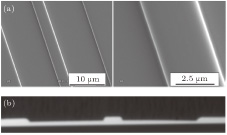 | Fig. 6. SEM images of (a) imprinted rib waveguide in As24Se38S38 chalcogenide glass and (b) cross sectional optical microscope view of waveguide. (Han et al. 2010)[24] |
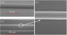 | Fig. 7. (color online) SEM images of the embossed As2S3 waveguides: (a) side wall image at 45°; (b) plan view of the embossed waveguide surrounded by depressed trenches; (c) magnified portion from panel (b) showing some roughening at the bottom of the rib. (Han et al. 2011).[25] |
Zou et al. (2013)[38] reported imprinted waveguides from thermally evaporated and solution deposited As2Se2 glass films by using hot-embossing. Optical loss in the waveguide fabricated from thermally evaporated film was measured to be 0.8 ± 0.3 dB/cm at 1550 nm, which is far lower than that in the waveguide from solution processed film (8.2 ± 0.6 dB/cm) by cut-back by using the optical fiber end-fire coupling. The higher loss in solution processed film is deemed to result from residual solvent absorption.[38] Abdel-Moneim et al. (2015)[23] reported the hot-embossing fabrication of low-loss, single-mode rib optical waveguide in RF-magnetron sputtered-deposited As2Se3 chalcogenide-glass thin film (core/under-clad: As2Se3/Ge17As18Se65; core: 4 μm–6 μm wide and 1.9 ± 0.1-μm high) [see Fig.
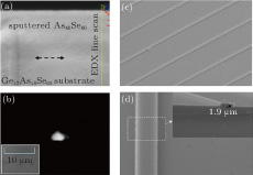 | Fig. 8. (color online) For the hot-embossing waveguide from RF-sputtered As–Se thin film on the pressed Ge–As–Se substrate: (a) ESEM cross-sectional image of a cleaved edge of an RF-sputtered As–Se thin film on the top of a Ge–As–Se substrate. (b) a near-field intensity profile observed at 1550-nm wavelength in the quasi-TE mode. SEM image of (c) top view of ribs and (d) one of the ribs at higher magnification, with a cross-sectional view sown in the inset. (Abdel-Moneim et al. 2015).[23] |
In Table
| Table 1.
Summary of the lowest recorded optical losses at 1550-nm wavelength for ChGs rib waveguides. The rib waveguides are shaped via hot embossing on either FOG or thermally evaporated, or RF-sputtered deposited, As–Se or As–S–Se films. . |
Hot embossing is an emerging lithographic technology that is faster, cheaper and more scalable. Especially, hot embossing is suitable for those materials with relatively low glass transition temperature like chalcogenide glasses with Tg around 100 °C–350 °C depending on the actual chemical compositions, and thus various microstructures on the surfaces of the materials can be easily created. There are several trials to fabricate low-loss ChGs waveguides by using hot embossing processing. Han et al. (2010)[24] reported the first low loss ChGs waveguides fabricated by hot-embossing in As24S38Se38 glass with a soft PDMS stamp. The optical loss was measured to be as low as 0.26 dB/cm at 1550 nm, which can be comparable to the best values obtained in waveguides fabricated by photolithography and dry etching. However, there are still some problems that remain to be solved: I) film decomposition, crystallization and surface evaporation or roughening may happen in the hot embossing process, and II) the sidewall structure of rib waveguide is likely to be damaged after film sample has been separated from the stamp. All these can lead to low quality waveguides. And currently, most selected film materials for hot embossing contain arsenic, which is detrimental to the environment. To overcome these problems, some solutions have been proposed: a) further selecting suitable ChGs film materials with high thermal stabilities and environment friendliness, i.e., Ge–Sb–Se system; b) coating the surface (SU-8, aluminium oxide or other ChGs film) to inhibit surface diffusion that contributes to the growth of the crystals on the surface of the core film; c) optimizing the preparation technology and trying to shorten the process of embossing at high temperature. Han et al.[25] have also reported that a hard h-PDMS layer is added on the surface of the softer PDMS stamp in order to increase the local rigidity and maintain global flexibility of the stamp, thereby improving the profile of the embossed waveguide.[39] In addition, it has been found that different film deposition methods have an effect on the quality of hot-embossing waveguides. For example, the optical loss of a hot-embossed rib waveguide (reported by Abdel-Moneim et al. 2015)[23] in an RF-magnetron sputter-deposited As40Se60 glass thin film on a Ge17As18Se65 glass substrate has been demonstrated to be lower than that in a hot-embossed mono-mode rib waveguide in a thermally-evaporated As40Se60 glass thin film, on a similar Ge17As18Se65 glass substrate.[22] The lower loss is believed to be due to a greater density and homogeneity of the ChGs film produced by RF-sputtering than by thermally-evaporation.[23] It is worth mentioning that the fabricating of nano-sized chalcogenide waveguides via hot embossing has not yet been reported so far, and therefore the future work on nano-size chalcogenide waveguide will be carried out to show the advantages of hot embossing technology.
| [1] | |
| [2] | |
| [3] | |
| [4] | |
| [5] | |
| [6] | |
| [7] | |
| [8] | |
| [9] | |
| [10] | |
| [11] | |
| [12] | |
| [13] | |
| [14] | |
| [15] | |
| [16] | |
| [17] | |
| [18] | |
| [19] | |
| [20] | |
| [21] | |
| [22] | |
| [23] | |
| [24] | |
| [25] | |
| [26] | |
| [27] | |
| [28] | |
| [29] | |
| [30] | |
| [31] | |
| [32] | |
| [33] | |
| [34] | |
| [35] | |
| [36] | |
| [37] | |
| [38] | |
| [39] |


