Hot-embossing fabrication of chalcogenide glasses rib waveguide for mid-infrared molecular sensing
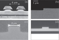
(a) SEM micrograph of a multilayer As24S38Se38/As2S3 rid waveguide processed by lithography and wet etching (Viens et al.).[
Hot-embossing fabrication of chalcogenide glasses rib waveguide for mid-infrared molecular sensing |
|
(a) SEM micrograph of a multilayer As24S38Se38/As2S3 rid waveguide processed by lithography and wet etching (Viens et al.).[ |
| |