1. IntroductionIt is generally known that one-dimensional (1D) semiconductor nanostructures are ideal systems for exploring basic physical properties at the nanoscale, such as quantum conductance, ballistic conduction, transformations and low thermal conductivity, which are of great importance for applications in nanophotonics and nanoelectronics.[1–5] More interestingly, when the sizes of such semiconductor structures diminish further, the resulting leap of specific surface area makes them much more sensitive and efficient for probing the surface chemical processes and optical signals around, as compared with their thicker counterparts which can significantly improve the performances of present chemical/biosensors and photodetective devices.[6–8] For instance, Hu et al. recently certified that the large specific surface area of small diameter SnO2 nanowires (NWs) can boosts the efficiency of the photodetectors.[9] Inspired by these virtues, the interest of developing small-sized 1D semiconductor nanomaterials has been culminated in the past few years.[10–12]
As a vital III–V semiconductor, 1D Indium Phosphide (InP) has demonstrated wide applications in electronic and optoelectronic fields for its natural merits, such as high carrier mobility, very low surface recombination velocity, and long carrier lifetime at room temperature.[13–16] Specially, this interesting material possesses a proper direct bandgap of 1.34 eV, which is proposed to be an attractive candidate for detecting visible radiation. Although many efforts have been devoted to the synthesis of 1D InP nanostructures systematically photoresponse investigations to date based on them are still limited.[17–20] More regrettably, the present works are generally focused upon the InP nanostructures of relatively large size, which did not allow full play to the advantages of 1D InP nanostructures in the photodetective field. Therefore, it is still highly desirable to develop high performance InP photodetectors based on the small-sized 1D nanostructures and conduct a comprehensive study of their working behaviors. In this work, small diameter InP NWs with high crystal quality and optical performances were successfully grown by a chemical vapor deposition (CVD) method, and field-effect transistors based on these individual InP NWs were built to study their electrical transport and photodetective properties. Benefitting from the high crystal quality and small diameter features of the NWs, a photodetector on the two-terminal configuration exhibited low power consumption and excellent light photoresponse, and the back-gate voltage dependent performance of the photodetectors was systematically investigated and explained using theoretical models. These succinct and high efficiency devices can expand the building blocks for high performance optoelectronic devices.
2. ExperimentsFor the growth of small diameter InP nanowire, the moving source CVD method was used (the experimental setup is shown in Fig. A1 in Appendix A). Typically, an alumina boat filled with 0.05 g InP powder (Alfa Aesar, 99.9999%) was first placed upstream and far enough from the center of the furnace, and several silicon wafers coated with 3 nm thick gold film were placed downstream at the deposition area. Before heating, Ar/H2 (15%) gas was introduced into the system at a rate of 50 sccm for 1 h, and the pressure was maintained at 3 Torr. The furnace was then heated to 780 °C (the substrate temperature was about 485 °C) for 3 mins to generate gold particles that served as catalysts for the growth of InP NWs. Then the boat with InP powder was shifted to the center of the furnace by a step motor. After 30 mins of growth, the furnace was naturally cooled down to room temperature. The as-grown NWs were characterized utilizing field emission scanning electron microscope (FE-SEM, Zeiss sigma-HD), atomic force microscopy (AFM, Brucker Bioscope System), x-ray diffraction (XRD) (Rigaku D/Max 2500) and a transmission electron microscopy (TEM, Tecai F20) equipped with energy-dispersive x-ray spectroscopy (EDX). Micro-photoluminescence (μ-PL) and Raman scattering spectra were carried out on a laser confocal Raman spectrometer (LABRAM-010, France) coupled with a continuous 632.8 nm laser for excitation.
Back-gate single NW field-effect transistors (FETs) were then fabricated. The as-obtained NWs were first dispersed in alcohol and then drop-cast onto the P+-Si/SiO2 (300 nm) wafers Cr/Au source and drain electrodes (5/65 nm) were defined by electron-beam lithography, metallization and lift-off process. The electrical transport measurements of FETs were conducted by the probe station combined with a semiconductor parameter analyzer (Keithley 4200-SCS). For photoresponse measurements, a power-tunable 520 nm semiconductor laser was used to provide incident light, while the time-dependent photocurrent were monitored by a current meter after switching on-off the illumination with a light chopper. All the measurements were conducted in air at room temperature.
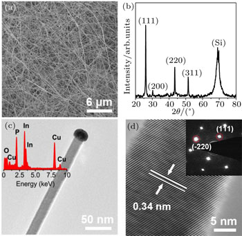
3. Results and discussion3.1. Morphology and structure characterizationAs demonstrated by a typical SEM image (Fig. 1(a)), large quantities of InP NWs with a length of about 50–80 μm were achieved on the substrate. Basically, the NWs have small diameters of 29.1 ± 8.3 nm, based on AFM studies (Fig. A2), suggesting a large specific surface area of the NWs. XRD pattern of the product (Fig. 1(b)) was indexed to the zinc blende (ZB) crystal (JCPDS: 65-233) without any detectable wurtzite (WZ) phase. A TEM image of a typical InP NW in Fig. 1(c) shows smooth sidewall and uniform diameter of about 25 nm along its entire length with a Au particle at the tip, indicating the vapor–liquid–solid growth mechanism.[21,22] The corresponding EDX spectrum inserted in Fig. 3(c) reveals that the NW consists of elements In and P with an equal ratio, very close to the stoichiometric value for a InP compound. Figure 1(d) represents a high-resolution TEM image recorded along the [112] zone axis. This image with the selected area electron diffraction (SAED) pattern inserted documents the high single-crystal quality with the ZB structure of our sample, and its growth direction is [111], which is consistent with the literature.[23]
3.2. Optical and electronic propertiesTo further investigate the nature of InP NWs, optical characterizations were performed. A typical PL spectrum recorded from a single NW in Fig. 2(a) shows the emission peak located at 870 nm (∼ 1.42 eV), indicating a blue-shift of 50 nm compared with the bulk ZB InP PL (920 nm), which is much more moderate with respect to the defects related emission.[24] This blue-shift can be explained by quantum confinement effect[25] correlated well with the average diameter of our samples. Figure 2(b) shows the first-order Raman scattering spectrum of a single InP NW. By means of Lorentzian fitting, the two strong peaks observed can be associated with the transverse optical (TO) mode at 301 cm−1 and the longitudinal optical (LO) mode at 339 cm−1. Comparing with the TO and LO modes of bulk InP, the detected modes in our nanostructure have 2 cm−1 and 6 cm−1 downshifts, respectively, which is ascribed to the quantum confinement effect as well.[26] In addition, the weak peak at 326 cm−1 probably originates from the surface optical (SO) mode as a consequence of fine size of the InP NW.[26] These results further confirm the high quality and the large specific surface area characteristics of the achieved InP NWs.
As illustrated in Fig. 3(a), back-gate single NW FETs were assembled to assess the electronic transport properties of the samples. Figure 3(b) shows the output characteristics of a representative device with a NW diameter of 30 nm and a channel length of 5.2 μm between two adjacent electrodes (a SEM image is shown in Fig. 3(a)). With the back-gate voltage (VGS) rising from −10 V to 10 V, the conductance of the device gradually increases, revealing a good gate-dependence. Meanwhile, the transfer characteristics were investigated at a low drain bias (VDS) of 0.1 V. As depicted in Fig. 3(c), the drain current (IDS) increases when the VGS mounts up, demonstrating a typical n-type semiconducting nature of the NWs, which is in agreement with the result observed by Hui et al.[27] In this study, the electron mobility μe of InP channel was derived from the transfer curve via the following formula:[28]

where d
IDS/(d
VGS) refers to the transconductance of the device, the value is calculated to be around 12 nS,
L is the channel length,
h (300 nm) and
d (30 nm) are the thicknesses of the dielectric SiO
2 layer and the NW diameter,
εr is the relative dielectric constant of SiO
2 and
ε is the permittivity of free space, respectively. As a result, the electron mobility was found to be 105 cm
2·V
−1·s
−1, which is comparable with the previous results.
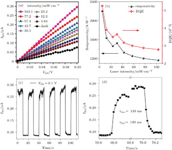
[20,27] 3.3. Photoresponse performancesBenefitting from the high mobility, the InP NWs can in principle be available for high performance photodetectors. We first measured its photoresponse properties under VDS = 0.1 V and VGS = 0 V on the two-terminal structure as displayed in Fig. 4(a) by turning 520 nm laser illumination with different power intensities ranging from to 103.1 mW/cm2. It can be observed that the drain current increases with the increased voltage, at the same time, it increases apparently with the increased light intensities. The spectral responsivity (Rλ) and external quantum efficiency (EQE) of the device can then be obtained by the following equations[29,30] Rλ = Iph/PS and EQE = Rλ hc/eλ, where Iph represents the photocurrent defined as the difference between light current and dark current (VDS = 0.1 V and VGS = 0 V), P and S (0.156 μm2) describe the corresponding light intensity and the effective illuminated area of the device, h refers to the Plank’s constant, c is the velocity of light, e is the electronic charge and λ is the incident light wavelength, respectively. An outstanding responsivity value of up to 2200 A·W−1 can be obtained at the intensity of 4.64 mW/cm2, although it trends a little downward when the laser intensity increases, the value of 1170 A·W−1 is still pretty high even at 103.1 mW/cm2, indicating an excellent conversion ability of optical to electrical signals and a low power consumption of the device (Fig. 4(b)). In addition, the achievable EQE value was estimated to be 2.80 × 10⁵% that can rival or even surpass the previous results.[17–20]
To explore the capability of the photodetector for fast-varying optical signals, the time-response cycles of the device were obtained by periodically turning on and off the laser at 10 s intervals, under incident laser intensity of 103.1 mW/cm2 at VDS = 0.1 V and VGS = 0 V. As plotted in Fig. 4(c), the device current rises up sharply and reaches to a steady state about 0.27 μA once the laser opened, and then falls down quickly to 0.08 μA when the light is blanked, demonstrating an excellent stability and reversible switching properties of the device. This good performance is confirmed by the longer-periodic time photoresponse measurements in Fig. A3. The rise time (τr) and fall time (τf), defined as the required time for the current rising to 90% and falling to 10% of the peak value, are about 110 ms and 130 ms, respectively, based on the enlarged curve in Fig. 4(d), which have comparability to the values improved by the ferroelectric-enhancing technique.[31] These good properties (both responsivity and response speed) are particularly attractive merits for optoelectronics and probably result from two unique characteristics of our NW samples. (i) The superior crystal quality. InP NWs with few defects benefit the transport of the carriers, thus increasing the photoconductive gain and facilitating the photocurrent to reach a steady state rapidly in both the rise and fall processes.[32,33] (ii) The small diameter of the NW (∼ 30 nm). On the one hand, the chemisorption around the NW becomes prominent as a result of the large specific surface area arising from its tiny structure. Consequently, adsorbates attached on the NW surface as hole-traps would prolong the lifetime of photo-generated carriers,[34] which guarantees the high photo-gain and responsivity of our device when light is turned on. On the other hand, as light is turned off, defects and dangling bonds at the NW surface could increase the recombination rate of carriers, meaning a shorter fall time.[35] In fact, both high responsivity and fast response speed imply that the surface trapping and recombination relaxation reach an equilibrium for the semiconductor channel.[36]
3.4. Effect of gate voltage on photoresponseAfterwards, we studied the effect of back-gate voltage on the performance of InP photodetectors. Figure 5(a) illustrates the plots of IDS versus VGS (VDS = 0.1 V) under different laser intensities as before. The conductivity of InP channel under illumination in both OFF and ON states increases effectively across the whole gate voltage range employed, indicating that photocurrent dominates over thermionic and tunneling currents across the entire operating range of gate voltages. Figure 5(b) plots the photocurrents with different VGS extracted from the transfer characterizations. Fitting the plots with power law of Iph ∼ Pθ,[35] we can extract the factor θ determining the efficiency of the photo-generated charges to light intensity as a function of VGS (−10 V to 10 V). At a low gate voltage of −10 V, a linear increase (θ = 0.98) of the photocurrent with the light intensity confirms that the photocurrent is solely determined by the amount of photo-generated carriers.[37] Whereas, when the gate bias further increases from −10 to 10 V at interval of 5 V, the device puts up a sublinear behavior, that is, the factor θ decreases monotonously with different values of 0.98, 0.92, 0.82, 0.74, and 0.65. The sublinear relation between the photocurrent and the laser intensity may relate to a complex photocurrent-generated mechanism.[34,35] Figure 5(c) shows the responsivity and EQE recorded as a function of gate voltage under illumination intensity of 103.1 mW/cm2 at 0.1 V bias, respectively. Similar to the modulation of channel conductivity, the gate voltage can bring a variation to the responsivity and EQE of InP photodetector. The responsivity of the device is only 138 A·W−1 when VGS = − 10 V, while VGS sweeping to 10 V, a preeminent value up to 1436 A·W−1 can be achieved and the EQE also increases by an order of magnitude. This gate-tunable property can provide the potential for the pixelated imaging applications.[38]
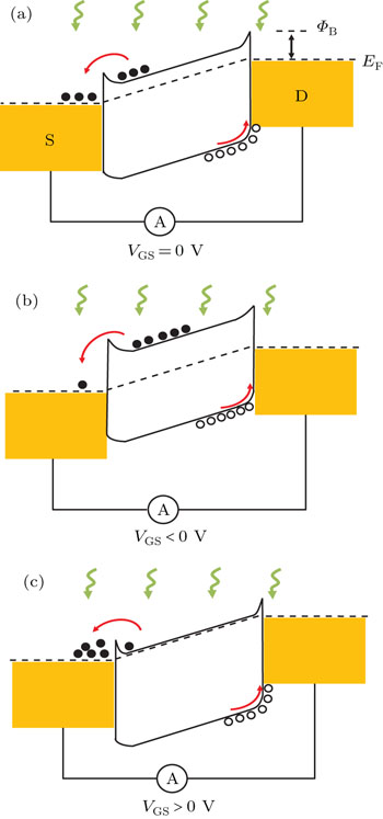
The above observed behaviors of our InP NW photodetectors can be explicated by a simple energy band diagram as depicted in Fig. 6.[31] As shown in Fig. 6(a), the InP device is in its quasi-equilibrium state under bias and illumination without back-gate voltage applied, which can be characterized by a small Schottky barrier at the interface between metal and semiconductor, where band tail drags especially slowly and depletion region extends deep into the channel.[39] When a negative gate voltage is applied, a larger barrier between InP and metal electrode occurs as compared to the state at zero gate voltage, hindering photo-generated carriers extraction by the applied bias voltage, thus leading to a low responsivity (Fig. 6(b)). Fortunately, since the width of depletion region can expand further with Schottky barrier increasing, the resulting strong local electric field in the semiconductor can separate the electron–hole pairs effectively, which guarantees a good dependence of the photocurrent.[40,41] At an extreme, the device photocurrent in the OFF state is merely determined by the photo-excited process and easily follows the linear relation to illumination intensity as described before in Fig. 5(b). Inversely, if the applied gate voltage is positive, the Schottky barrier can be lower, allowing more efficient photo-response for the device (Fig. 6(c)).[42] However, the narrow depletion region cannot separate the electron–hole pairs effectively, which consequently easily deviate the relationship between photocurrent and illumination intensity from linear to sublinear dependence.
4. ConclusionIn summary, we have realized the synthesis of small diameter (less than 30 nm) and high crystallinity InP NWs that possess excellent optical properties. Electrical transport measurements of the nanostructures show a high electron mobility of 105 cm2·V−1·s−1. Benefitting from large specific surface area and high crystallinity character of the NWs, the as-fabricated photodetector exhibits good sensing performance, such as a responsivity of 1170 A·W−1, external quantum efficiency of 2.8 × 10⁵% and fast response speed (τr = 110 ms, τf = 130 ms). In addition, the back-gate voltage related photoresponse of the device was investigated, which can be explicated by a simple energy band diagram. These findings may accelerate the progress of a new generation of optoelectronic devices.


