Large scale fabrication of nitrogen vacancy-embedded diamond nanostructures for single-photon source applications
Jiang Qianqing1, 4, 5, Li Wuxia1, †, , Tang Chengchun1, Chang Yanchun1, 5, Hao Tingting1, 5, Pan Xinyu1, Ye Haitao3, Li Junjie1, Gu Changzhi1, 2, 5, ‡,
Beijing National Laboratory of Condensed Matter Physics, Institute of Physics, Chinese Academy of Sciences, Beijing 100190, China
Collaborative Innovation Center of Quantum Matter, Beijing 100190, China
School of Engineering and Applied Science, Aston University, Birmingham B4 7ET, United Kingdom
Beijing National Laboratory for Molecular Sciences, Institute of Chemistry, Chinese Academy of Science, Beijing 100190, China
CAS Key Laboratory of Vacuum Physics, School of Physical Sciences, University of Chinese Academy of Sciences, Beijing 100190, China


† Corresponding author. E-mail: liwuxia@iphy.ac.cn

‡ Corresponding author. E-mail: czgu@iphy.ac.cn

Project supported by the National Key Research and Development Plan of China (Grant No. 2016YFA0200402), the National Natural Science Foundation of China (Grants Nos. 11574369, 11574368, 91323304, 11174362, and 51272278), and the FP7 Marie Curie Action (project No. 295208) sponsored by the European Commission.

Abstract
Abstract

Some color centers in diamond can serve as quantum bits which can be manipulated with microwave pulses and read out with laser, even at room temperature. However, the photon collection efficiency of bulk diamond is greatly reduced by refraction at the diamond/air interface. To address this issue, we fabricated arrays of diamond nanostructures, differing in both diameter and top end shape, with HSQ and Cr as the etching mask materials, aiming toward large scale fabrication of single-photon sources with enhanced collection efficiency made of nitrogen vacancy (NV) embedded diamond. With a mixture of O2 and CHF3 gas plasma, diamond pillars with diameters down to 45 nm were obtained. The top end shape evolution has been represented with a simple model. The tests of size dependent single-photon properties confirmed an improved single-photon collection efficiency enhancement, larger than tenfold, and a mild decrease of decoherence time with decreasing pillar diameter was observed as expected. These results provide useful information for future applications of nanostructured diamond as a single-photon source.

1. Introduction

Diamond is an important material with many outstanding properties that serve as the basis for its applications in biology, high-pressure science, and other fields.[17] Benefiting from its abundant naturally existing or artificially induced color centers, the material now draws more and more interest from researchers globally for its heretofore unobserved physical and optical properties and promising applications in areas such as single-photon source, high-sensitivity sensors, and information processing.[820] Of particular interest is the electron spin of nitrogen vacancy (NV) centers in diamond, which can be initialized, coherently controlled, and read out at room temperature.[11] The robust spin coherence[13] and optical addressability via spin-dependent orbital transitions[14] strongly suggest that such systems have great potential in applications ranging from quantum information processing[1518] to nanoscale magnetic field sensing.[2124]

However, bulk diamond crystals have the disadvantage of low photon out-coupling, that is, the total reflection effect at the diamond–air interface results in tremendous loss of fluorescence photon counting rate. To address this problem, theoretical and experimental works have been performed to investigate the effects of size and geometry on the single-photon collection efficiency of NV-embedded diamond structures. In particular, different micro/nano structures like hemispheres and nanowires have been fabricated out of diamond substrates to improve the in- and out-coupling of photons, to facilitate the manipulation of the light–matter interactions,[2527] and for more efficient excitation, higher collection efficiency, and single-photon flux.[28] For size effect studies, thin and high-aspect-ratio nanowires covered with a graphic or carbonaceous shell have been obtained through chemical vapor deposition (CVD).[29] Diamond fibers with various diameters were fabricated by a top-down method and the best shape for diamond nanowires was predicted by simulations. The optical coupling of the NV center emission (at λ = 637 nm) to diamond nanowire has been modeled using FDTD simulations.[30] The best coupling efficiency was found in nanowires with diameters between 180 nm and 220 nm.[31,32] In addition, in recent work, the effect of a nanowire's morphology on single-photon collection efficiency was reported for a conical nanowire, and a net photon flux exceeding 1.5 × 10⁶ s−1 was achieved.[32] Nevertheless, optimized fabrication approaches for large scale diamond micro-/nano-structures with tunable geometry, size, and distribution are still much needed.[33]

For the work reported in this paper, we adopted a two-stage technique of electron beam lithography (EBL) followed by induction coupled plasma (ICP) reactive ion etching (RIE) to fabricate diamond nanopillars of various sizes and top shapes. Thin diamond nanopillars with diameters down to 45 nm and aspect ratios up to 20 were prepared. The nanopillar top end geometry evolution process during etching was studied systematically. The dependency between the fluorescence photon collection rate of the NV center and the nanopillar's diameter was also probed. Measurement of the single-photon count rate indicates an enhancement of about tenfold in photon collection efficiency compared with the un-sculpted diamond crystal. The g(2)(τ) and Ramsey fringe measurements show that the RIE processing affects neither the single-photon emission nor the coherence properties. The size effect was examined and the underlying mechanism is discussed.

2. Methods

Two alternative kinds of fabrication processes, HSQ negative resist (Fig. 1(a)) and PMMA positive photoresist (Fig. 1(b)), were adopted in the experiment. For the former, first, HSQ was spin-coated on a cleaned diamond surface. Then electron beam lithography (EBL) was performed. For EBL processing, the accelerating voltage was set to 100 keV, and the dose varied with the pattern size. For circles larger than 80 nm in diameter, the applied dose was 1600 μC/cm2. For smaller circles, the applied dose was 2500 μC/cm2. After developing, the silicon oxide pattern was used as a mask for the subsequent reactive ion etching (RIE) treatment, in which a gas mixture of CHF3: O2 (4.2 sccm: 30 sccm) was used. During the RIE procedure, the chamber pressure was 10 mTorr and the RF power was 100 W. After RIE etching, the remaining mask material was wiped off in diluted HF solution and the diamond nanopillars were finally obtained.
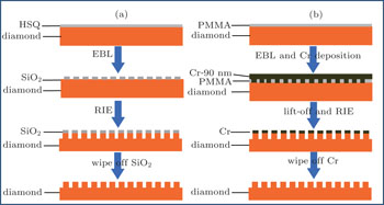
Fig. 1. Top-down fabrication of diamond nanostructure arrays by electron beam lithography related techniques: (a) HSQ negative resist approach, (b) PMMA positive resist approach.

For the PMMA approach, again, a layer of 300 nm PMMA was spin-coated on a cleaned diamond surface. Then circle patterns were exposed with EBL and developed. Thereafter, Cr was deposited, 90 nm thick, with a thermal evaporation system, followed by lift-off in acetone to obtain circular Cr masks. Unlike the first approach, rather than using the developed resist as the mask, here we used a pattern transfer process, metal deposition, and lift-off. After RIE processing, the remaining Cr was removed to leave diamond nanopillars.

The measurements of fluorescence scanning and single-photon count rate were carried out on a home-built laser scanning confocal microscope system that can detect single-photon fluorescence with sub-micrometer precision. During measurement, a 532-nm continuous wave laser beam was switched on and off by an acoustic optical modulator (AOM); an XY galvanometer was used to control the scanning of the laser spot before it was directed to the sample through a microscope objective. The spin state-dependent fluorescence of the NV center was collected by the same objective, which was then filtered by a 532 nm notch and a 650 nm long path. After that, the weak light signal was translated into an electronic pulse signal by a single-photon counting module and was subsequently counted by a pulse counter or routed to a Hanbury–Brown and Twiss detection system to record the second order intensity correlation function g(2)(τ).

3. Results and discussion
3.1. Fabrication of diamond nanostructure arrays

Diamond nanopillar arrays of various diameters and periods have been prepared with the HSQ approach. First of all, the effect of the period of the patterns was examined. For a particular diameter, patterns with the period set twice, threefold, fivefold, and tenfold were prepared. For the developed masked cylinders of small diameter, we found that only arrays of small periods can stand straight. Specifically, pillars with diameter of 50 nm or 80 nm easily “fall down” on the substrate when the period is larger than three times the diameters. Figure 2(a) shows the array of 50 nm diameter pillars with a period of 100 nm, which stands well. For pillars wider than 100 nm, the period can be set larger, as shown in Fig. 2(b), the pillars are 300 nm in diameter and the period is 1.5 μm.
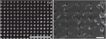
Fig. 2. Pillars prepared with the HSQ negative resist approach: (a) diameter 50 nm, period 100 nm; (b) diameter 300 nm, period 1.5 μm. The scale bar is 2 μm.

With the PMMA approach, several Cr-masked column arrays of different diameters and different periods were prepared. Arrays of pillars with diameter of 80 nm, period of 160 nm and diameter of 250 nm, period of 500 nm are shown in Fig. 3. Compared with the PMMA approach, pillars prepared with HSQ have better cylindrical shape and their diameter can be smaller, since the Cr mask size is limited by the lift-off process, which has a minimum diameter of 80 nm.

Fig. 3. Pillars prepared with the PMMA positive resist approach: (a) diameter 80 nm, period 160 nm; (b) diameter 250 nm, period 500 nm. The scale bar is 2 μm.

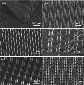
Diamond nanopillar arrays of different diameters and different periods were then prepared in an RIE system employing HSQ (Fig. 4) and PMMA (Fig. 5), respectively. It should be mentioned that ultra-thin diamond nanopillars with diameter of 45 nm, period of 100 nm, and height of about 900 nm were prepared with the HSQ approach (Fig. 4(a)). The length-diameter ratio reached as high as 20. For pillars of such small diameter, the maximum array period should not exceed twice the diameter of the masks, otherwise, the resulting pillars easily fall down. Pillar arrays of 100 nm and 500 nm in diameter were prepared with HSQ, as shown in Figs. 4(b) and 4(c). It is clear that they all have a conical top-end. Here we would like to point out that the EBL technique is well known for its high resolution, repeatability, and controllability in the sub-10 nm realm. Notice also that less than 3 h was required to fabricate an array of nanopillars 250 nm in diameter and 500 nm in period in an area of 1.0 mm × 1.0 mm using an exposure electron beam current of 1.0 nA, which is practical in most occasions.

Fig. 4. Pillars fabricated with the HSQ negative resist approach having diameters and periods of: (a) 50 nm, 100 nm; (b) 100 nm, 500 nm; (c) 220 nm, 500 nm; (d) 730 nm, 1.5 μm; (e) 500 nm, 1.5 μm; (f) 1.0 μm, 2.0 μm.

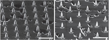
Diamond nanopillars prepared with the PMMA approach also have a conical top-end (Fig. 5). From Figs. 5(a) and 5(b), in which the periods are both 1.5 μm, while the diameters are 300 nm and 250 nm, respectively, it can be seen that the apex angle is smaller for thinner pillars.

Fig. 5. Cone structure on the top end of the pillars: (a) diamond pillar array of diameter 300 nm, period 1.5 μm, fabricated with the HSQ approach; (b) diamond pillar array with pillar diameter of 250 nm, period 1.5 μm, fabricated through the PMMA approach. The scale bar is 2 μm.

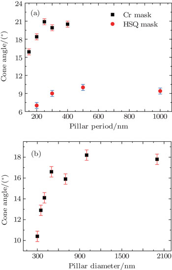
To find out the relationship between the apex angle and the mask material, a more detailed experiment was undertaken. The apex angles of the pillars prepared with both Cr and HSQ masks were measured as shown in Fig. 6. All the pillars are 100 nm in diameter in Fig. 6(a). It is clear that the apex angle of the pillars with a certain diameter increases with the period up to a certain maximum value. We attribute this phenomenon to the etching rate, which is closely related to the mask pattern density. When the pillars stand closely, the incident ions are scattered by the etched structures and strike the nearby pillars, which may hinder the formation of the apex angle.

Fig. 6. Apex angle variation. (a) Effects of mask type and mask pattern period. The measured pillars are 100 nm in diameter. (b) Effect of mask diameter. Here the pillar period is three times that of the pillar diameter.

It should also be noted that the apex angle of the pillars prepared by the HSQ approach has a smaller range of increase − – the maximum value is just half that of those prepared with a Cr mask. Such a difference comes mainly from the initial tomography of the two mask materials. By comparing the HSQ mask results and Cr mask results shown in Figs. 2(b) and 3(b), respectively, we can see that the HSQ pillars have a steep sidewall while the Cr pillars already have an apex angle. In the subsequent etching process, the apex angle was gradually enlarged and the initial difference was kept or even magnified. Larger apex angles were finally obtained for pillars fabricated with Cr masks. The variation of apex angle with pillar diameter was further studied with the pillars fabricated using HSQ as the etching mask, and the pattern period was three times the diameter. As shown in Fig. 6(b), the apex angle increases with the pillar diameter up to an angle of about 18°, at which it is maximized.

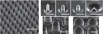
For a better understanding, the apex angle evolution during the etching process was investigated and a simple model was proposed. At first, diamond pillar arrays of different diameters were etched using the PMMA approach in which the Cr mask was used (Fig. 7(a)). With all residual mask material removed, long-time etching was undertaken, during which the top-end apex angle of the pillars was checked at 70 min, 130 min, 160 min, and 310 min of the process. For pillars of 200 nm in diameter, SEM images of different etching times are shown in Figs. 7(b) and 7(c). As can be seen from these images, the top-end apex angle was unchanged after it had been formed on the pillar, while the pillar height gradually decreased as the etching went on. For a pillar of 1 μm diameter, the apex angle was enlarged when the etching time was changed from 70 min to 310 min, as shown in the SEM image of Figs. 7(f) and 7(g). As mentioned before, the residual mask material was removed after 70 min etching, which means the subsequent etching was undertaken on pre-formed pillars with no mask.

Based on the experimental results discussed above, we here propose a conical top end evolution model of diamond pillars prepared by RIE. The process is roughly divided into three stages (Fig. 8). At the initial stage, with the bombarding of incident reactive ions, a small facet forms at the edge of the masked cylinder, shown as inclined line AB in Fig. 8(a), and a truncated-top cone appears. As the etching continues, the facet expands and the apex angle increases till the pillar is cone shaped (Fig. 8(b)). Then the tapered facets go down into the diamond pillar at a certain etching rate, till the end of the etching process or the mask material is totally etched away (Fig. 8(c)).

Fig. 7. Effect of the etching time on the top shape of pillars: (a) diamond pillar array fabricated with the PMMA approach; (b)–(e) tomographic evolution of a 200 nm diameter pillar when the etching time was 70 min, 130 min, 160 min, and 310 min; (f), (g) tomographic evolution of a 1 μm diameter pillar when the etching time was 70 min and 310 min, respectively. The scale bar is 500 nm.

The conical shape forms earlier for pillars of smaller diameter than for the thicker ones. The apex angle of the latter keeps increasing while the former one becomes fixed. In this way, larger apex angles can be obtained for thicker pillars, as we discussed with regard to Fig. 6(b). When we removed the mask from the top end at 70 min etching, a conical shape had already formed on small pillars (Fig. 7(b)) while larger ones still had a circular truncated conical top end (Fig. 7(f)). The apex angle would remain fixed for the former, while it would continue to expand for the latter.

Fig. 8. The top shape evolution process of the etched pillars: (a) facet forming at the edge of a cylinder; (b) expansion of the facet on the etched pillar; (c) formation of the conical top end.
3.2. Single-photon properties of nanostructured diamonds

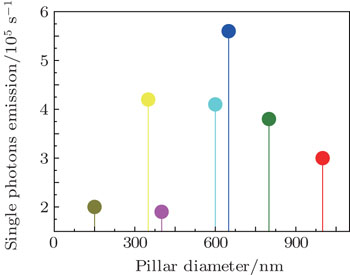
For measuring single-photon properties, pillars with diameter from 150 nm to 1 μm were prepared on a piece of 1 ppm diamond with proper distribution of single NV centers by the HSQ approach. In the confocal scanning imaging process, obvious brighter spots can be picked out, their positions can be identified, and they can be confirmed to represent NV-center emissions. The second order autocorrelation function measurement further verified the single-photon emission property. The relation between the single-photon collection efficiency enhancement and the diameter of the pillar was then studied. Pillar arrays of various diameters were scanned and their single-photon counting rates were compared. The single-photon counting rates of NV centers in pillars with a given diameter vary. We take pillars of 800 nm diameter as an example, the largest counting rate was 3.8×10⁵ counts/s, while the smallest was 2.7×10⁵ counts/s. The inset of Fig. 9 gives the largest measured counting rate of NV centers in pillars with each diameter value from 150 nm to 1 μm. The highest enhancement, about 10 folds, was obtained at 650 nm diameter, which differs from the simulation results in the previous report,[5] while the relation between the counting rate and the diameter is not that obvious. We attribute this result to the pillar shape, which has a conical top end fabricated with the RIE system, and the randomness of the NV center position in the pillars, which may depart from the pillar center.

Fig. 9. Single NV center emission count rate for pillars of different diameters.

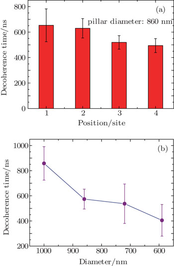
Decoherence time measurements were then taken on pillars of varied diameters. The of NV center clusters in different pillars of the same diameter differs as the circumstances inside/outside the pillars varies. For instance, the of NV center clusters in 860 nm pillars at room temperature ranges between 500 ns and 700 ns (Fig. 10(a)). In our experiment, several pillars of the same diameter were measured at room temperature, and the average value of was taken to make a contrast between pillars of different diameters. It turns out that of NV center clusters in diamond nanopillars decreases with the pillar diameter (Fig. 10(b)). This dependence can be attributed to the circumstances near the diamond pillar surface. During pillar etching, reactive ions bombard the pillar surface, which may introduce a large number of defects such as atom replacement and vacancies to a certain depth into the pillar. Together with dangling bonds on the pillar surface, these defects alter the local electromagnetic environment of the NV centers near the pillar surface and disturb the electron spin of the centers, which finally reduces the of the centers. As the pillar diameter decreases, a greater proportion of the NV centers are distributed near the pillar surface, in which case defects near the pillar surface can make greater impact. Therefore, we observed decreased for centers with reduced pillar diameters. This observation implies that by the EBL related mask fabrication method, abundant nano-diamond structures could be fabricated. However, since the distribution of the naturally formed NV centers in diamond is random, the exact location of the NV centers is hard to control. To address this issue, self-aligned masking by EBL related patterning is considered as a potential approach.[34] In that method, EBL would first be employed to design the sites on the diamond structure for every individual NV center; then implantation/doping would be conducted, followed by self-masked dry etching. Consequently, every diamond nanostructure could have one NV center embedded, and the effective NV centers would be far more valuable for practical applications.

Fig. 10. (a) Decoherence time of NV center clusters in four diamond pillars of 860 nm in diameter. (b) Pillar diameter dependent average decoherence time.
4. Conclusion

We show effective fabrication of diamond nanopillars of varied diameters with both HSQ and PMMA approaches using RIE. Ultra-thin pillars of 45 nm in diameter and high/diameter ratio of 20 were obtained with the HSQ approach. We find that a conical top end can be formed and the apex angle changes with the mask material, the mask period, and the diameter of the pillars. A facet-etching model is then proposed to explain the top shape evolution. The size dependent single-photon collection efficiency of NV centers buried in the diamond pillars was investigated. It was found that the best enhancement exceeded tenfold. The measurement also shows variation of the decoherence time of pillars with the same diameter, which might be correlated with the shape of every pillar and the random distribution of the site position of each NV center in different pillars. However, a mild decrease of decoherence time with reduction of pillar diameter has been observed, which is as expected. Our results could provide very useful information for future applications of nanostructured diamond as single-photon sources.

Reference
1Brookes C A 1970 Nature 228 660
2Faklaris OJoshi VIrinopoulou TTauc PSennour MGirard HGesset CArnault J CThorel ABoudou J PCurmi P ATreussart F 2009 Acs Nano 3 3955
3Luo DWu LZhi J 2009 Acs Nano 3 2121
4Li LXu JXu L FLi J JWang J TGu C Z 2015 Chin. Phys. 24 056803
5Liu A PLiu MYu J CQian G DTang W H 2015 Chin. Phys. 24 056804
6Chen J YZheng H FZhang HWeng K NZeng Y S2005Physics34221(in Chinese)
7Fang CJia X PYan B M 2015 Acta Phys. Sin. 64 0228101
8Maze J RStanwix P LHodges J SHong STaylor J MCappellaro PJiang LDutt M VTogan EZibrov A SYacoby AWalsworth R LLukin M D 2008 Nature 455 644
9Robledo LChildress LBernien HHensen BAlkemadeP FHanson R 2011 Nature 477 574
10Bernien HChildress LRobledo LMarkham MTwitchen DHanson R 2012 Phys. Rev. Lett. 108 043604
11Kurtsiefer CMayer SZarda PWeinfurter H 2000 Phys. Rev. Lett. 85 290
12Jelezko FGaebel TPopa IGruber AWrachtrup J 2004 Phys. Rev. Lett. 92 076401
13Balasubramanian GNeumann PTwitchen DMarkham MKolesov RMizuochi NIsoya JAchard JBeck JTissler J 2009 Nat. Mater. 8 383
14Gruber ADrab̈enstedt ATietz CFleury LWrachtrup JBorczyskowski C 1997 Science 276 2012
15Dutt M VChildress LJiang LTogan EMaze JJelezko FZibrov A SHemmer P RLukin M D 2007 Science 316 1312
16Neumann PBeck JSteiner MRempp FFedder HHemmer P RWrachtrup JJelezko F 2010 Science 329 542
17Buckley B BFuchs G DBassett L CAwschalom D D 2010 Science 330 1212
18Robledo LChildress LBernien HHensen BAlkemade P F AHanson R 2011 Nature 477 574
19Zhang QShi F ZDu J F 2015 Physics 44 565
20Zhang X ZWang K YLi Z HZhu Y MTian Y MChai Y S 2015 Acta Phys. Sin. 64 0247802 (in Chinese)
21Maze J RStanwix P LHodges J SHong STaylor J MCappellaro PJiang LDutt M V GTogan EZibrov A S 2008 Nature 455 644
22Balasubramanian GChan I YKolesov RAl-Hmoud MTsisler JShin CKim CWojcik AHemmer P RKrueger A 2008 Nature 455 648
23Dolde FFedder HDoherty M WNob̈auer TRempp FBalasubramanian GWolf TReinhard FHollenberg L C LJelezko F 2011 Nat. Phys. 7 459
24Liu G BSunX PGu S HFeng J WZhou X2012Physics41803
25Hausmann B J MKhan MZhang YBabinec T MMartinick KMcCutcheon MHemmer P RLončar M 2010 Diam. Relat. Mater. 19 621
26Baik E Sbaik Y JLee S WJeon D 2000 Thin Solid Films 377 295
27Tao YDegen C 2013 Adv. Mater. 25 3962
28Babinec T MHausmann B JKhan MZhang YMaze J RHemmer P RLoncar M 2010 Nat. Nanotech. 5 195
29Hsu C HXu J 2012 Nanoscale 4 5293
30Hausmann B J MKhan MZhang Y 2010 Diamond and Related Materials 19 621
31Hausmann B J MBabinec T MChoy J T 2011 J. Phys. 13 045044
32Momenzadeh S AStoöhr R Jde Oliveira F F 2014 Nano Lett. 15 165
33Castelletto SHarrison J PMarseglia LStanley-Clarke A CGibson B CFairchild B AHadden J PHo Y L DHiscocks M PGanesan KHuntington S TLadouceur FGreentree A DPrawer SO'Brien J LRarity J G 2011 New J. Phys. 13 025020
34Toyli D MWeis C DFuchs G DSchenkel TAwschalom D D 2010 Nano Lett. 10 3168