† Corresponding author. E-mail:
Project supported by the National Natural Science Foundation of China (Grant Nos. 61574110, 61574112, and 61106106).
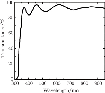
AZO-gated and Ni/Au-gated AlGaN/GaN HEMTs are fabricated successfully, and an excellent transparency of AZO-gated electrode is achieved. After a negative gate bias stress acts on two kinds of the devices, their photoresponse characteristics are investigated by using laser sources with different wavelengths. The effect of photoresponse on AZO-gated electrode device is more obvious than on Ni/Au-gated electrodes device. The electrons are trapped in the AlGaN barrier of AZO-gated HEMT after it has experienced negative gate bias stress, and then the electrons can be excited effectively after it has been illuminated by the light with certain wavelengths. Furthermore, the trap state density DT and the time constant τT of the AZO-gated Schottky contact are extracted by fitting the measured parallel conductance in a frequency range from 10 kHz to 10 MHz. The constants of the trap range from about 0.35 μs to 20.35 μs, and the trap state density increased from 1.93 × 10¹³ eV−1·cm−2 at an energy of 0.33 eV to 3.07 × 10¹¹ eV−1·cm−2 at an energy of 0.40 eV. Moreover, the capacitance and conductance measurements are used to characterize the trapping effects under different illumination conditions in AZO-gated HEMTs. Reduced deep trap states' density is confirmed under the illumination of short wavelength light.
AlGaN/GaN heterostructure transistor is considered as a great candidate in power and switching applications due to its high saturation electron velocity and high breakdown voltage[1,2] Al-doped ZnO (AZO) has many important applications in transparent electronics.[3,4] The transparent gate AlGaN/GaN HEMT has promising applications in transparent electronics. Evaluation of trap characteristics can be implemented on transparent gate device illuminated by light. Recently, the AZO-gated AlGaN/GaN HEMT with excellent characteristics[5,6] and the Ni/ITO-gated AlGaN/GaN HEMTs[7] have been reported. The photosensing characteristics have been reported on AZO-gated AlGaAs/InGaAs HEMTs.[8] However, few results are reported on the photoresponse and trap characteristics of transparent gate AlGaN/GaN HEMT. Thus, the effects of light illuminating on saturation current and trap states characteristic need further studying.
In this paper, the AZO-gated AlGaN/GaN HEMT is fabricated. After introducing the traps charging under the action of negative gate bias stress, the photoresponse of the device is investigated compared with the conventional Ni/Au-gate device on the same epitaxial structure. Moreover, the constants of the trap and the trap states density are extracted by capacitance and conductance measurements in a frequency range from 10 kHz to 10 MHz. In addition, the conductance measurements under the illumination with different wavelengths are also investigated.
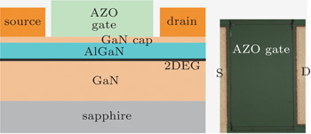
The large-size gate electrode device, named FAT-FET, is used for investigating transparent gate electrode characteristics, which is shown in Fig.
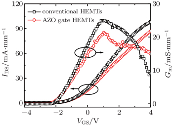
The transfer characteristics and the transconductance characteristics of the AZO-gated HEMTs and Ni/Au-gated HEMTs are shown in Fig.
In order to study the photoresponse characteristics of the AlGaN/GaN HEMT with AZO transparent gate electrode, the experiment with electric stress and illumination on AZO-gated HEMT is performed, and the conventional Ni/Au-gated HEMT is also employed for comparison. The stress bias was VG = −40 V, VD = 0 V, VS = 0 V for 100 s for the off-state. After being experienced by the negative gate bias stress, the HEMT is placed in the dark for 100 s and then the slight change of saturation current is observed, indicating that the effect of stress on saturation current cannot recover rapidly with increasing time. Stressing and measuring in a certain illumination each time, may be considered as a circle. After being stressed each time, the device is placed in the ambient of blue, green and red light for measuring, respectively. I–V characteristics in different ambient conditions are measured. The wavelengths of red light, green light and blue light are 650 nm, 532 nm, and 405 nm, respectively. The total test results are shown in Figs.
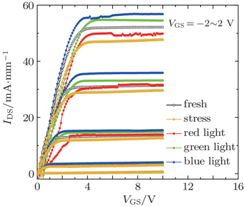 | Fig. 4. IDS–VDS characteristics of the AZO-gated HEMTs with electric stress under different illumination conditions. |
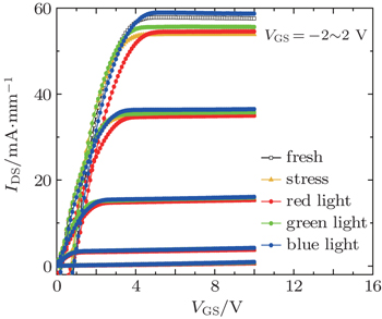 | Fig. 5. IDS–VDS characteristics of the Ni/Au-gated HEMTs with electric stress under different illumination conditions. |
As can be noted in Figs.
In order to investigate the recoveries of two kinds of devices after being stressed, three lasers with varying wavelengths are employed to illuminate the gate electrodes. In the case of AZO-gated HEMT, compared with the output saturation current after being stressed for 100 s, Ids values with the red light, green light, and blue light illuminations are increased by 4.3%, 14.9%, and 19.1%, respectively. The Ids values after green and blue light illuminations exceed the output current in the fresh state. As for Ni/Au-gated HEMTs, compared with the output saturation current under post-stressing condition, Ids values with the red light, green light, and blue light illuminations are increased by 1.9%, 3.8%, and 9.4%, respectively. Under the illumination condition, the output saturation current of the two devices is increased, but the magnitudes of the rise are different. It reveals that the trapped electrons can obtain energy by illumination, so the excited electrons will escape from the traps and the electron concentration in the channel is increased.[9] In addition, photon-generated carriers are induced by illumination, so that the electron concentration in the channel is even more than the normal concentration. However, 10 min later after removing illumination, the Ids reaches its fresh state, which indicates the recombination of photon-generated carriers. Furthermore, because the gate region of the AZO-gated HEMT is transparent, the light can easily transmit it, and therefore the photoresponse is more sensitive, which is beneficial to investigating the trap characteristics of the region underneath the gate as mentioned by Pei et al.[7] Thus, frequency-dependent capacitance and conductance measurements are performed to analyze the AZO-gated HEMTs.
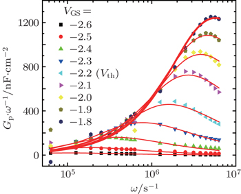
Figure
According to the fitting results, the time constant of the trap state as a function of the gate voltage is plotted in Fig.
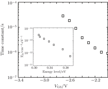 | Fig. 7. Trap state time constant as a function of gate voltage, with the inset showing trap state density as a function of their energy. |
The trap state energy can be calculated by using time constant τT = (σT NcνT)−1 exp(ET/kT), in which the trap state capture cross section σT = 3.4 × 10⁻¹⁵ cm−2, the effective density of states of conduction band Nc = 2.2 × 1018 cm−3, and the average velocity of thermal motion of carrier νT = 2.6 × 107 cm/s are used. The trap state density as a function of energy level is shown in the inset in Fig.
In order to further study the trap characteristics of transparent AZO-gated HEMT the interface state analysis and comparison are carried out under the illumination condition. The capacitance and conductance measurements in a frequency range from 10 kHz to 10 MHz are utilized to characterize the trapping effects under different illumination conditions. With the 5-min illumination of light with different wavelengths, the fitting results of the test data measured from CV variable-frequency scanning are shown in Fig.
 | Fig. 8. Plots of trap state time constant versus (a) gate voltage and (b) energy level, with the illuminations of different-wavelength light. |
As figure
AlGaN/GaN high-electron-mobility transistors (HEMTs) with AZO transparent gate electrodes are fabricated and investigated. The effect of photoresponse on AZO-gated electrode device is more obvious than that of Ni/Au-gated electrode device. The capacitance and conductance measurements in a frequency range from 10 kHz to 10 MHz are utilized to characterize the trapping effects under different illumination conditions in AZO-gated HEMTs. The quantitative analysis results of the trap density and time constant are obtained. Under different illumination conditions in AZO-gated HEMTs, the reduction of the deep trap density is founded in illumination of the shorter wavelength.
| 1 | |
| 2 | |
| 3 | |
| 4 | |
| 5 | |
| 6 | |
| 7 | |
| 8 | |
| 9 | |
| 10 | |
| 11 | |
| 12 | |
| 13 | |
| 14 |


