Modeling of trap-assisted tunneling on performance of charge trapping memory with consideration of trap position and energy level
Lun Zhi-Yuan1, Li Yun1, Zhao Kai2, Du Gang1, †, , Liu Xiao-Yan1, Wang Yi1
Institute of Microelectronics, Peking University, Beijing 100871, China
School of Information and Communication, Beijing Information Science and Technology University, Beijing 100101, China


† Corresponding author. E-mail: gangdu@pku.edu.cn

Project supported by the National Natural Science Foundation of China (Grant Nos. 61404005, 61421005, and 91434201).

Abstract
Abstract

In this work, the trap-assisted tunneling (TAT) mechanism is modeled as a two-step physical process for charge trapping memory (CTM). The influence of the TAT mechanism on CTM performance is investigated in consideration of various trap positions and energy levels. For the simulated CTM structure, simulation results indicate that the positions of oxide traps related to the maximum TAT current contribution shift towards the substrate interface and charge storage layer interface during time evolutions in programming and retention operations, respectively. Lower programming voltage and retention operations under higher temperature are found to be more sensitive to tunneling oxide degradation.

1. Introduction

In the past few years we have seen the explosive growth of the non-volatile semiconductor memory market because of the unceasing demand for higher memory density and lower bit cost.[1] During the aggressive scaling of flash memory technology, the floating gate structure has faced great challenges from both technological and physical limitations, such as reducing coupling ratio, cell-to-cell interference, and increasing gate leakage current.[2] In order to continue the scaling trend, great effort has been devoted to developing next-generation memory structures.[36] Among these structures, the charge trapping memory (CTM) shows the most excellent potential as one of the most promising candidates for future memory solutions.[79] Furthermore, in recent years, high-density CTM in three-dimensional (3D) architectures for the NAND applications has drawn a great deal of attention.[1012]

Under this circumstance, understanding the physical mechanisms in CTM has growing importance in terms of designing and optimizing CTM devices. The trap-assisted tunneling (TAT) is one of the most important mechanisms influencing the memory performance. On the one hand, TAT is an indispensable part of the tunneling current due to the existence of intrinsic defects in oxide layers. An accurate calculation of TAT current is crucial for achieving high accuracy in modeling CTM performance. On the other hand, it is largely accepted that electrical stress in the tunneling oxide during program/erase (P/E) cycle leads to the generation of interface defects and bulk traps in oxide layers.[13,14] In this regard, the TAT mechanism is related to reliability issues of the memory cells after P/E cycle, leading to a variation of memory characteristics. Especially, degradation in tunneling oxide can cause the increase in charge loss during retention operation. However, previous studies on modeling the TAT mechanism mainly focused on the gate leakage current of the MOS structure.[1517] Only little work has addressed the TAT effect in the context of flash memory cells.[18,19]

In this paper, the TAT mechanism in CTM cells is carefully modeled and implemented in the developed simulator[2022] for NAND flash memory. The influence of the TAT mechanism on CTM performance is investigated in consideration of various oxide trap positions and energy levels. The programming and retention performances of CTM after P/E cycle are also evaluated.

2. Physical model and simulation approach

The device structure we used to evaluate the influence of TAT on CTM performance is a standard CTM cell with 4.5-nm/6-nm/10-nm (SiO2/Si3N4/Al2O3) gate stacks as shown in Fig. 1.
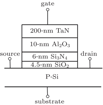
Fig. 1. Schematic illustration of the simulated standard CTM cell with a 4.5/6/10 nm (SiO2/Si3N4/Al2O3) gate stack.

The TAT mechanism is modeled as a two-step process,[23] i.e., the electron capture and emission of the oxide traps. The TAT current driven through each oxide trap is given by the capture and emission times for each trap, τc,ch/csl and τe/csl respectively, considered from the charge reservoir, i.e., channel or charge storage layer as schematically illustrated in Fig. 2.
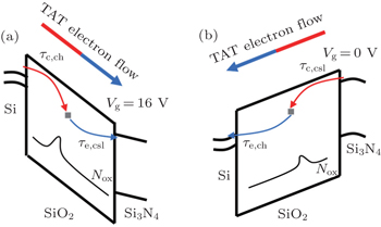
Fig. 2. Schematics of the capture and emission time constants for calculating TAT current in (a) programming and (b) retention operations.

Accumulating the current-density contributions from the traps in a small interval dx at each distance x, the total TAT current density through the entire oxide layer is expressed as

where tox is the thickness of oxide layer and Nox is the volume density of oxide traps with respect to distance in tunneling oxide. Solving device electrostatics and current continuity equations in our CTM memory simulator allows the calculation of these time constants, which is based on an SRH-like model[24] with considering the spatial and energetic locations of the oxide traps and the charge reservoir. Here we calculate the time constants for a single acceptor-like oxide trap and assume that it only interacts with the conduction band of the channel and the charge storage layer. The capture and emission time constants are described by the following equations:

where fn is the electron energy distribution function in the reservoir and gn is the density of states. The processes of electron capture and emission are described by energy-dependent capture and emission coefficients cn and en. With regard to the distribution function, the Fermi–Dirac distribution is assumed, and has the useful property,

where

In addition, according to the SRH theory,[25] the correlation between capture and emission coefficients is

with ET being the energy level of the oxide traps.

It should be mentioned that the calculations of capture and emission coefficients are related to the energetic position of ET with respect to the energy level E in the integration. When ET is lower than E, the capture coefficient is energy-independent and can be written as

where υth is the thermal velocity of electron, σ0 is the capture cross section, and θ is the elastic tunneling coefficient between the reservoir and the oxide trap calculated in the WKB approximation. When the ET is higher than E, the emission coefficient rather than the capture coefficient should be energy-independent.

In order to improve calculation efficiency, an approximation is made to solve the above complicated integral by assuming E = Ec for calculating the time constants.[24] Overall, using Eqs. (1)–(6), we can rewrite the capture and emission time constants as follows:

where Nc is the density of states in the conduction band and εc and εe are the capture and emission barriers which are determined by

The abovementioned physical model accounting for the TAT mechanism has been incorporated into our calibrated two-dimensional (2D) self-consistent CTM simulator,[21] which carefully takes into consideration the DT/FN tunneling process, charge trapped/de-trapping mechanisms, and drift-diffusion transport in the gate stack of memory cells. In addition, oxide traps with arbitrary energy level and spatial distribution are considered in the simulation. The main parameters adopted in the simulation are summarized in Table 1.[26,27]

Table 1.

Main parameters for the simulation.

.
3. Results and discussion

In order to obtain an overview of the influences of the TAT mechanism on programming and retention characteristics of CTM cells, we first perform the simulations in the cases with and without considering the TAT effect. In addition to the TAT mechanism, in the simulation the direct and FN tunneling process within the tunneling oxide are taken into consideration. Comparisons between simulation prediction and experimental measurement are also made. Figure 3 shows a good reproduction of experimental data[27] for all programming voltages considered. A uniform spatial distribution of traps is assumed for the charge storage layer, under a trap density of Nt = 7 × 1019 cm− 3 and a trap cross section σn = 1 × 10− 14 cm2. The trap density is an important factor in determining the memory window,[28] and hence is obtained from fitting the experimental characteristics. For the simulation of TAT contribution, we consider typical parameters for oxide defects in accordance with those reported previously[29] for thermally grown oxides. The intrinsic trap distribution across the tunneling oxide is assumed to be uniform under an oxide defect density of Nox = 3 × 1016 cm− 3, a trap energy level around 2 eV, and a trap cross section of σT = 8 × 10− 14 cm2. For the simulated memory cell, the interface traps located at tunneling oxide borders are not included in the simulation. It can be seen that without considering the TAT current, the programming speed is underestimated and simulations and measurements are not in agreement with each other. In addition, the role played by TAT current is found to be non-negligible at lower oxide fields: lower programming voltages, and larger occupation of the traps in the charge storage layer (longer programming time). Using the same material parameters for the charge storage layer and slightly modified parameters for intrinsic oxide defects (Nox = 2 × 1016 cm− 3 and σT = 5 × 10− 14 cm2), good agreement between experimental retention measurements[30] and simulations under a wide variety of temperatures can be achieved as shown in Fig. 4. The result indicates that modeling the TAT mechanism is also crucial in predicting retention characteristics, which can lead to extra charge loss from the charge storage layer.
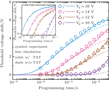
Fig. 3. Comparison between experimental programming data and simulation results of CTM cells and influence of TAT on programming characteristics.
Fig. 4. Comparison between experimental retention and simulation predictions of CTM cells under different temperatures and influence of TAT on retention characteristics.

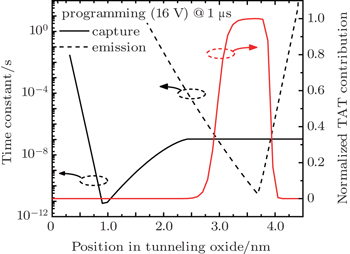
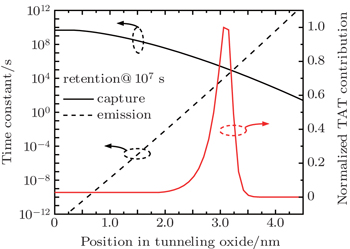
The defect traps allow an extra tunneling path in the oxides, but not all traps have equivalent contribution to TAT current. From Eq. (1), it is known that capture and emission time constants are used to calculate TAT current density of each oxide trap. Figure 5 shows the variations of capture and emission time constants and normalized TAT current contributions with position along tunneling oxide under 16-V programming voltage at 1 μs for the simulated device. It is found that only the oxide traps in a small distance (approximately 1 nm) at the position of 3.5 nm from the substrate interface make the main contribution to the overall TAT current. Similarly, figure 6 shows the variations of capture and emission time constants and normalized TAT contribution with position along tunneling oxide for 375 K retention simulation at 107 s. Oxide traps located within a length of 0.2 nm at the position of 3 nm from the substrate interface are related to major TAT current.

Fig. 5. Capture and emission time constants used to calculate TAT current density along tunneling oxide and the related normalized TAT current contribution under 16-V programming voltage at 1 μs.
Fig. 6. Capture and emission time constants used to calculate TAT current density along tunneling oxide and the related normalized TAT current contribution for 375-K retention simulation at 107 s.

However, the positions of peak contribution to the overall TAT current are variable with time evolution under programming and retention operations as shown in Fig. 7. In the programming process, the shape of the curve for normalized TAT contribution becomes narrower with time evolution. Simultaneously, the position of the maximum contribution shifts towards the substrate interface. In comparison, the shape of the curve keeps unchanged with the peak shifting towards the charge storage layer interface during retention. The variation in positions of the maximum contribution can be ascribed to the movement of band edge in different phases of the programming and retention operations.
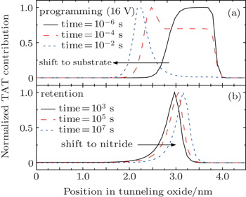
Fig. 7. The variations of normalized TAT contribution with position in tunneling oxide with time evolution in (a) programming and (b) retention operations.

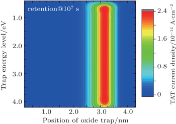
Apart from the position of oxide defects, trap energy level is another major factor to determine TAT current. To investigate the influences of the trap energy level and spatial position on TAT current density, we assume that the trap distribution in tunneling oxide has a Gaussian distribution with a peak value of 7 × 1018 cm− 3 and a small standard deviation of 0.2 nm. Simulations of devices with various peak positions and trap energy levels are performed. Figure 8 shows the TAT current density under 16-V programming voltage at 1 μs of a device with a 4.5/6/10 nm gate stack (SiO2/Si3N4/Al2O3). The oxide traps located around 1 nm from the oxide/nitride interface with lower energy level are related to larger TAT current density. Figure 9 shows the TAT current densities of devices with various peak oxide trap positions and energy levels at 107 s of retention under 360 K temperature. It is shown that oxide traps located at 1.4 nm from the oxide/nitride interface are related to the maximum TAT current density, which has little dependence on the trap energy level ranging from 0.6 eV to 4.0 eV.
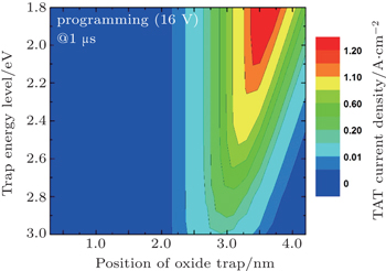
Fig. 8. TAT current densities under 16-V programming voltage at 1 μs of devices with various peak positions and trap energy levels.
Fig. 9. TAT current densities at 107 s of retention operation under 360-K temperature of devices with various peak positions and trap energy levels.

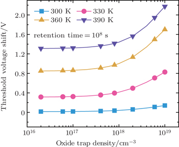
During P/E operations, the electric field in tunneling oxide can typically exceed 10 MV/cm.[31] A Large number of P/E cycles leads to the generation of oxide traps and thus causes reliability issues of CTM cells. The influences of TAT on programming and retention operations are strongly correlated with trap density in tunneling oxide. Figure 10 shows the programming speeds under different programming voltages with increasing the level of tunneling oxide degradation. A unanimous programming window of 5 V is used for all cases. It can be seen that programming under lower voltage is more sensitive to oxide degradation. Figure 11 shows the threshold voltage shift after 108 s under various retention temperatures with increasing the level of tunneling oxide degradation. Higher temperature is found to be more sensitive to oxide degradation.

Fig. 10. Programming speeds under different programming voltages with increasing the level of tunneling oxide degradation.
Fig. 11. Threshold voltage shifts after 108 s under various retention temperatures with increasing the levels of tunneling oxide degradation.
4. Conclusions

In this paper, we carefully model TAT mechanism in CTM cells and evaluate the influences of TAT on programming and retention characteristics. Our results indicate that the TAT mechanism is a critical factor for CTM operations, especially at low tunneling oxide fields. The influence of the TAT mechanism on CTM performance is investigated in consideration of various trap positions and energy levels in the tunneling oxide.

The results show that only the oxide traps at a small distance are related to a major contribution to TAT current. In addition, the positions corresponding to the maximum contribution shift towards the substrate interface and the charge storage layer interface during programming and retention operations, respectively. Lower programming voltage and retention operations under higher temperature are more sensitive to tunneling oxide degradation.

Reference
1White M HWang YWrazien S JZhao Y 2006 Int. J. High Speed Electron. Syst. 16 479
2Ielmini DSpinelli A SLacaita A LModelli A 2001 Microelectron. Eng. 59 189
3Meena J SSze S MChand UTseng T Y 2014 Nanoscale Res. Lett. 9 1
4Hou YCelano UGoux LLiu LFantini ADegraeve RYoussef AXu ZCheng YKang JJurczak MVandervorst W 2016 Appl. Phys. Lett. 108 123106
5Chen JDu GLiu X Y 2015 Chin. Phys. 24 057702
6Fan XChen H PWang QWang Y QLv S LLiu YSong Z TFeng G MLiu B 2015 Chin. Phys. Lett. 32 068301
7Park YChoi JKang CLee CShin YChoi BKim JJeon SSel JPark JChoi KYoo TSim JKim K 2006 Proceedings of International Electron Devices Meeting 1
8Gilmer D CGoel NPark HPark CVerma SBersuker GLysaght PTseng H HKirsch P DSaraswat K CJammy R 2009 Proceedings of International Electron Devices Meeting 1
9Liu L FPan L YZhang Z GXu J 2015 Chin. Phys. Lett. 32 088501
10Tanaka HKido MYahashi KOomura MKatsumata RKito MFukuzumi YSato MNagata YMatsuoka YIwata YAochi HNitayama A2007Proceedings of Symposium on VLSI Technology141514–510.1109/VLSIT.2007.4339708
11Jang JKim H SCho WCho HKim JShim S IJang YJeong J HSon B KKim D WKihyun Shim J JLim J SKim K HYi S YLim J YChung DMoon H CHwang SLee J WSon Y HChung ULee W S2009Proceedings of Symposium on VLSI Technology192193192–3
12Park K TByeon D SKim D H2014Proceedings of the 14th Non-Volatile Memory Technology Symposium151–510.1109/NVMTS.2014.7060840
13Lun ZWang TZeng LZhao KLiu XWang YKang JDu G2013Proceedings of International Conference on Simulation of Semiconductor Processes and Devices292295292–510.1109/SISPAD.2013.6650632
14Fayrushin ALee C HPark YChoi J HChung C 2013 IEEE Trans. Electron Dev. 60 2031
15Larcher L 2003 IEEE Trans. Electron Dev. 50 1246
16Vianello EDriussi FEsseni DSelmi Lvan Duuren M JWiddershoven F2006Proceeding of the 36th European Solid-State Device Research Conference403406403–610.1109/ESSDER.2006.307723
17Zhang MHuo ZYu ZLiu JLiu M 2011 J. Appl. Phys. 110 114108
18Lee KKang MSeo SKang DLi D HHwang YShin H 2014 Electron Dev. Lett. 35 51
19Amoroso S MGerrer LAdamu-Lema FMarkov SAsenov A2013Proceedings of International Reliability Physics Symposium3B.4.13B.4.63B.4.1–3B.4.61610.1109/IRPS.2013.6531980
20Peng YLiu XDu GLiu FJin RKang J 2012 Chin. Phys. 21 078501
21Lun ZDu GZhao KLiu XWang Y 2016 Sci. China: Inf. Sci.
22Song YLiu XDu GKang JHan R 2008 Chin. Phys. 17 2678
23Gerrer LMarkov SAmoroso S MAdamu-Lema FAsenov A 2012 Microelectron. Reliab. 52 1918
24Grasser T 2012 Microelectron. Reliab. 52 39
25Shockley WRead W T 1952 Phys. Rev. 87 835
26Vandelli LPadovani ALarcher LSouthwick R GKnowlton W BBersuker G 2011 IEEE Trans. Electron Dev. 58 2878
27Padovani ALarcher LHeh DBersuker G 2009 Electron Dev. Lett. 30 882
28Seo Y JKim K CKim H DJoo M SAn H MKim T G 2008 Appl. Phys. Lett. 93 063508
29Padovani ALarcher LVerma SPavan PMajhi PKapur PParat KBersuker GSaraswat K2008Proceedins of International Reliability Physics Symposium616620616–2010.1109/RELPHY.2008.4558955
30Padovani ALarcher LHeh DBersuker GDella M VPavan P 2010 Appl. Phys. Lett. 96 223505
31Moon PLim J YYoun T UPark S KYun I 2014 Solid-State Electron. 94 51