
Nanoscale control of low-dimensional spin structures in manganites
[Wang Jing1, Ahmed Malik Iftikhar1, Liang Renrong2, Huang Wen3, Zheng Renkui4, Zhang Jinxing1, †,  ]
]
]
|
|


† Corresponding author. E-mail:
Project supported by the National Basic Research Program of China (Grant No. 2014CB920902), the National Natural Science Foundation of China (Grant Nos. 61306105 and 51572278), the Information Science and Technology (TNList) Cross-discipline Foundation from Tsinghua National Laboratory, China and the Fund from the State Key Laboratory of Electronic Thin Films and Integrated Devices, University of Electronic Science and Technology of China, Chengdu 610054, China.
Due to the upcoming demands of next-generation electronic/magnetoelectronic devices with low-energy consumption, emerging correlated materials (such as superconductors, topological insulators and manganites) are one of the highly promising candidates for the applications. For the past decades, manganites have attracted great interest due to the colossal magnetoresistance effect, charge-spin-orbital ordering, and electronic phase separation. However, the incapable of deterministic control of those emerging low-dimensional spin structures at ambient condition restrict their possible applications. Therefore, the understanding and control of the dynamic behaviors of spin order parameters at nanoscale in manganites under external stimuli with low energy consumption, especially at room temperature is highly desired. In this review, we collected recent major progresses of nanoscale control of spin structures in manganites at low dimension, especially focusing on the control of their phase boundaries, domain walls as well as the topological spin structures (e.g., skyrmions). In addition, capacitor-based prototype spintronic devices are proposed by taking advantage of the above control methods in manganites. This capacitor-based structure may provide a new platform for the design of future spintronic devices with low-energy consumption.
For the last few decades, transition metal oxide materials have attracted intensive research interest due to the novel physical properties and the potential applications in next-generation electronic/magnetoelectronic devices. Very recently, there emerges a variety of novel quantum materials such as high-temperature superconductors,[1] topological insulators,[2] and multiferroics[3] whose spin, charge, orbital, and lattice degrees of freedom strongly interact with one another. Among these materials systems, peroverskite LaMnO3 with chemical doping, generally defined as “manganites”, have attracted intensive attention because they exhibit a variety of interesting phenomena, including metallic ferromagnetic (FM), orbital- (OO) and charge-ordered (CO) antiferromagnetic (AFM), and complex electronic phase separation and spin-glass states,[4] etc. In manganites, the A sites are usually occupied by trivalent rare-earth elements (e.g., La, Pr, Nd, etc.) and alkaline-earth elements such as Ca, Sr, Ba. To maintain the charge balance, a portion of Mn3+ ions were oxidized to Mn4+ions, resulting in the coexistence of mixed valance state of the manganese ions. Due to the variant Mn3+/Mn4+ ratio, manganites show multiple electrical and magnetic phase transitions as a function of temperature,[5] such as metal–insulator, order–disorder, FM–AFM transitions), which are very sensitive to external stimuli (e.g., pressure, magnetic or electric fields[6]).
The discovery of colossal magnetoresistance (CMR) effect[7] (a distinct change of resistivity under the application of external magnetic fields) usually results from the magnetic-field-induced insulator-to-metal[6–9] and/or structural phase transitions.[10] Up to now, the fundamental microscopic origin of CMR effect is still under debate, the role of the double-exchange (DE) interaction, FM/AFM super-exchange interaction, charge/orbital ordering instabilities as well as their strong coupling with lattice deformation are not well understood.[11–14] In addition, the CMR effect can only exist at extreme conditions (low temperature, high magnetic field), which are technically impractical and thus restrict the possible applications. Furthermore, the modulation of CMR effect by chemical doping[15] could not achieved reversibly. Therefore, it gives people a push to find a way of the deterministic control of order parameters in manganites at nanoscale, especially at ambient conditions.
Very recently, manganites with unique magnetic domain patterns and topological spin configurations[16–19] attract people’s interest. In this review, we introduce the recent work about nanoscale control of spin structures at phase boundaries, domain walls with novel topological spin configurations including skyrmions in manganites using microscopy techniques. Through a full understanding of the dynamics of the low-dimensional spin structures, a capacitor-based spintronic device is proposed, in which writing and reading processes are correlated to the dynamics of phase boundaries, domain walls, and skyrmions in manganites, respectively. We hope this concept would provide a new platform in the development of new-generation spintronic devices with lower power consumption.
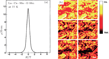
In 1950, the existence of ferromagnetism driven by DE interaction in manganites was discovered by Jonker and Van Santen.[20,21] Afterwards,Wollan and Koehler reported the coexistence of FM and AFM phases in La1−xCaxMnO3 using neutron scattering technique.[22] In 1994, Jin et al. discovered a huge negative magnetoresistance (MR) effect around 77 K in epitaxial La0.67Ca0.33MnOx thin films, exhibiting a high MR value of 1.27 × 10⁵% under the application of 6-T magnetic field (Fig.
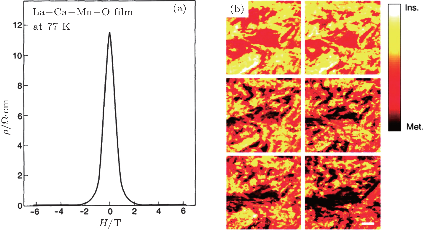 | Fig. 1. CMR effect and phase separation in La0.67Ca0.33MnOx and La0.73Ca0.27MnO3 epitaxial thin films. (a) A resistivity (ρ) versus magnetic field (H) curve obtained from La0.67Ca0.33MnOx epitaxial thin films grown on LaAlO3 substrate at 77 K and the MR ratio reaches to 1.27 × 10⁵%. (b) STS images of the local electronic structure of (La, Ca)MnO3 thin film taken just below Tc in magnetic fields of 0, 0.3, 1, 3, 5, and 9 T (from left to right and top to bottom). Parts of the surface are insulating (light colors), whereas others are metallic (dark colors) or in an intermediate state. The color represents the local differential conductance at a fixed bias of 3 V. Scale bar, 100 nm. (a)Reprinted with permission from Ref. [7]. Copyright 1994, The American Association for the Advancement of Science. (b) Reprinted with permission from Ref. [28]. Copyright 1999, The American Association for the Advancement of Science. |
Nevertheless, the underlying microscopic mechanism for CMR effect is not fully understood. The double-exchange interaction,[11,21,23,24] electron–phonon coupling,[21] and electronic phase separation[14,25] play partial roles on the CMR effects. Furthermore, the ground states of manganites tend to be intrinsically inhomogeneous due to the presence of strong phase separation, typically involving FM metallic and AFM CO/OO insulating phases.[14] Based on the intrinsic phase-separation properties of manganites, the formation of percolative paths for manganese eg electrons through FM regions was proposed by Uehara et al.,[26] who demonstrated that the (La,Pr,Ca)MnO3 system electronically phase separated into a sub-micrometer-scale mixture of FM metallic and CO insulating regions and percolative transport through FM domains depends sensitively on relative spin orientation of adjacent FM domains, which can be controlled by applied magnetic fields. In the following years, researchers demonstrated phase separation and percolative transport in manganites by transport and microscopy measurements[27–33] with a spatial resolution. These results shed new light on the microscopic origin and the nanoscale control of the CMR effect in manganites.
In 1999, Fäth et al. firstly presented real-space images of the mixed phases of La0.7Ca0.3MnO3 thin films across a metal–insulator transition (MIT) using scanning tunneling microscopy (STM) and scanning tunneling spectroscopy (STS). Local electronic properties were spatial inhomogeneous on a sub-micrometer scale in La0.7Ca0.3MnO3 thin film (Fig.
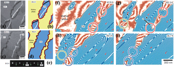
Although extensive theoretical and experimental studies have shown that the percolative connection of FM regions is the essential mechanism that gives rise to the CMR effect,[26–33] it is still unclear how FM phase prevails under the strong competition with CO phase, e.g., how phase boundaries evolve under application of magnetic field. In 2009, Y. Murakami et al. demonstrated magnetic-field-induced nucleation and growth of an ordered FM phase in the La0.25Pr0.375Ca0.375MnO3 thin films by directly observing the dynamics of phase boundaries and flux distributions using cryogenic Lorentz microscopy and electron holography. The boundary between FM and CO phases and the coalescence of FM domains were independent on the mother phase in zero-field-cooling process (Fig.
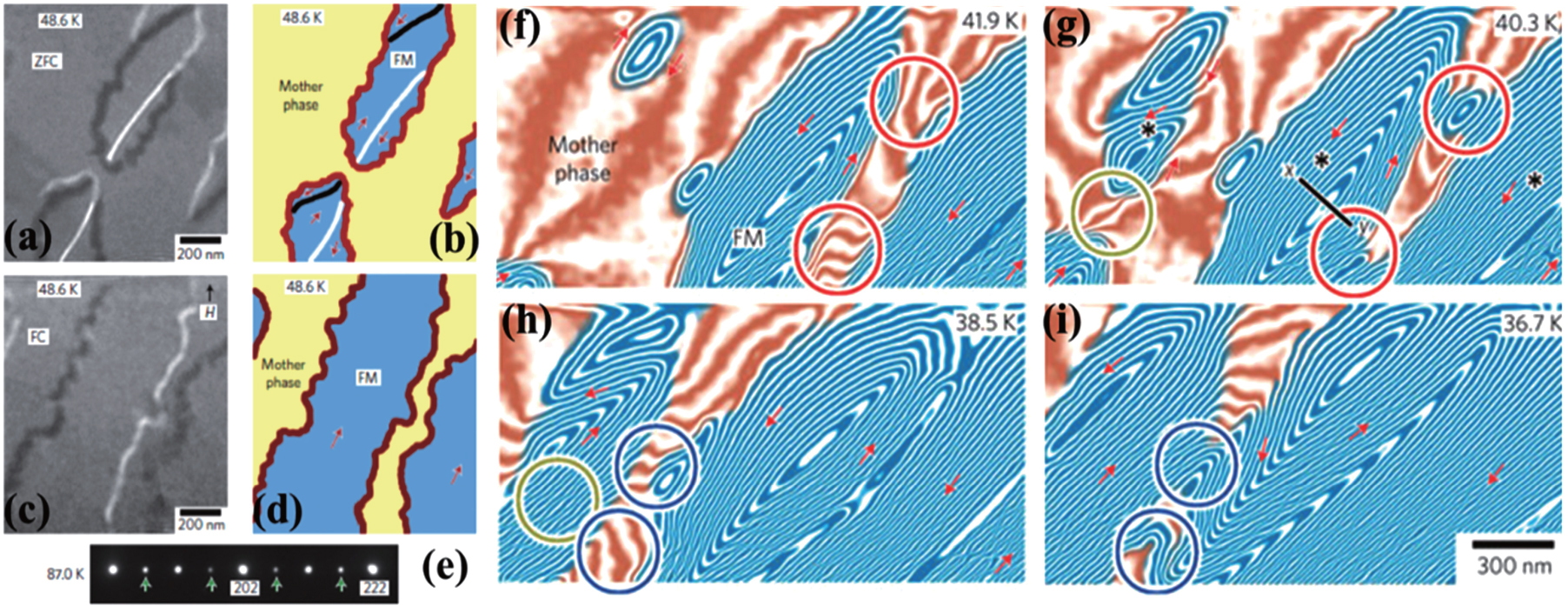 | Fig. 2. Microscopic observation of phase boundaries and the coalescence of FM domains using cryogenic Lorentz microscope and electron holography. Lorentz microscope images of multiple domains and a single domain formed in ZFC (a) and FC (c). (b), (d) The corresponding schematics of the boundary structures in panels (a) and (c). The red lines in panels (b) and (d) depict the phase boundaries, and the black and white lines in panel (b) represent the magnetic domain walls within multiple FM domains. The red arrows in panels (b) and (d) indicate the magnetization vectors determined by the holographic analysis. The black arrow in panel (c) represents the direction of the applied magnetic field H in the FC measurement. The Lorentz microscope images were taken in the under-focus condition. (e) Electron diffraction pattern observed in the mother phase at 87 K. The green arrows indicate superlattice reflections, which indicate the presence of the CO portions within the mother phase. (f)–(i) ZFC observations of the coalescence of FM domains distributed independently in the mother phase. Regions having blue lines are in the FM phase and those having sepia lines are in the mother phase. Contour lines and the red arrows represent the in-plane component and the direction of the magnetic flux, respectively. Domain connection occurs preferentially in areas (indicated by circles) where the leakage magnetic field is relatively strong. The phase information has been amplified by a factor of four. The red circles, green circles, and blue circles represent domain coalescence that was observed in cooling from 41.9 K to 40.3 K, from 40.3 K to 38.5 K, and from 38.5 K to 36.7 K, respectively. Reprinted with permission from Ref. [32]. Copyright 2009, Nature Publishing Group. |
Spin-polarized-current-induced magnetic DW motion in transition metal nanowires has attracted great research interest because of the nontrivial physical properties[34–40] and the potential applications in memories/registers.[41,42] The intrinsic driving force for the DW motion is the spin transfer torque (STT). Nevertheless, the obstacle that prevents the real application of the DW motion is the serious heating effect induced by the high threshold current density. In order to meet the requirement of low energy consumption in spintronic devices,[42–45] researchers have tried to explore multiple ways to reduce the threshold current density such as novel geometries[46] and techniques.[47–49] In 2011, Chanthbouala et al. reported higher efficiencies of intrinsic torques on domain walls by taking advantage of the geometry of vertical-current injection as compared with that of planar-current injection. The out-of-plane (‘field-like’) torque plays a major role on DW displacement in the case of vertical-current injection, which is consistent with theoretical calculations. The involved current densities are about 100 times smaller than that commonly observed with in-plane currents.[46] Later, Koyama et al. reported that the threshold current density for DW motion in a perpendicularly magnetized Co/Ni nanowire was determined by intrinsic pining, and thus the adiabatic spin torque dominates in DW motion. This conclusion was supported by the field-independent threshold current density and the presence of its minimum on tuning the wire width.[47]
Though people have attempted to explore the nontrivial physics and spin-torque efficiency, there is no dramatic breakthrough for the low threshold current density in transition metals, which is a significant ingredient to power consumption of future spintronic devices and registers based on DW motion. Therefore, one question arises: is there any possibility to achieve DW motion with lower current density in other magnetic materials? In recent years, several groups have studied current-driven magnetization switching and DW motion in transition metal oxides and semiconductors. Yamanouchi et al. demonstrated that magnetization reversal through DW switching in an FM semiconductor can be induced in the absence of a magnetic field using current pulses with densities below 109 A/m2.[50] Feigenson et al. reported magnetic DW motion in sub-micrometer patterns of FM SrRuO3 films with current density in the range of ∼ 109–1010 A/m2, which is ∼ 2–3 orders of magnitude smaller than the one in transition metals, indicating relatively high spin-torque efficiency in this oxide thin film.[51] However, the slow switching speed and low FM transition temperature limit the practical application of these materials.
Apart from the motion of nanoscale phase boundary and their role on the CMR effect, manganites may also be a good model system for the magnetic DW motion driven by low current density during the STT process. Compared with 3d transition metals, complex oxides such as La0.7Sr0.3MnO3[52–54] inherently exhibit a high spin polarization P[55] and a low saturation magnetization Ms, which is promising for applications of current-driven DW motion, due to a spin-torque efficiency that scales as P/Ms.[56] In 2014, Foerster et al.[57] studied the interaction between spin-polarized current and magnetization on La2/3Sr1/3MnO3 (LSMO) nanowires with in-plane anisotropy using low temperature magneto-transport method. A magnetic domain wall was nucleated in the area between the electrical contacts of the ring structure indicated by higher resistance for angles between 10° and 25°, as shown in Fig.
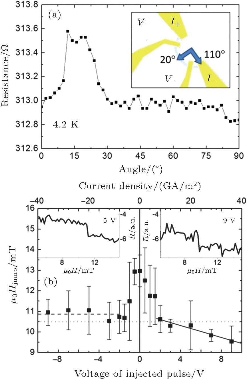 | Fig. 3. DW injections and depinning in LSMO half ring with in-plane anisotropy. (a) Resistance of LSMO half ring as a function of the angular of DW position. The increase of the resistance for directions between 10° and 25° (see inset) indicates a magnetic domain wall is positioned between the two inner contacts of the wire. (b) DW depinning fields in LSMO half ring as determined from the jump in the resistance signal. Data shown is averaged over six measurements in different experimental runs each, with error bars corresponding to one standard deviation. The lines correspond to different fits of high current density data (assuming either symmetric or asymmetric behavior). The insets show examples of two depinning field measurements for 5 V and 9 V pulses, showing also the increase in the resistance fluctuations. Reprinted with permission from Ref. [57]. Copyright 2014, AIP Publishing LLC. |
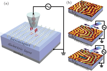
Very recently, Wang et al. the reported probe-induced magnetic DW motion in LSMO thin films with perpendicular anisotropy, which was integrated in a manganite/dielectric/metal capacitor (Fig.
 | Fig. 4. A probe-based ferromagnet/dielectric/metal capacitor for spin displacement and magnetic DW motion in FM layer after the application of scanning probe bias. (a) Contact geometry of vertical spin displacement between a downward-magnetized (red thick arrow) tip and a domain wall in aferromagnet/dielectric/metal capacitor. (b) The domain patterns before (top panel) and after the application of an AC voltage on a scanning tip once(intermediate) and twice (bottom panel) at the same area. The colored lines indicate the movement along the fast-scanning direction. Scale bar, 400 nm. Reprinted with permission from Ref. [59]. Copyright 2014, American Physical Society. |
Skyrmion,[60] a vortex-like topological spin texture where the spins were predicted to be in all directions wrapping a sphere, is recently discovered in B20-type helimagnets[18,19,61–65] as seen in their temperature/magnetic-field (T/B) phase diagram. In these systems, DM interaction naturally leads to a helical (HL) spin order, which turns into a triangular skyrmion crystal (SkX) under an external magnetic field[66,67] as observed in a narrow region of the B–T phase diagram for bulk samples by neutron-scattering experiments.[62] One characteristic of B20-type helimagnets is that they lack space inversion symmetry, which is believed to be a key ingredient of magnetic skyrmions.[62,67,68] Enhanced stability of the SkX in two-dimensional (2D) systems or in thin-plate samples was predicted theoretically,[69] and indeed confirmed by Lorentz microscope experiments.[68,70,71] Skyrmion configuration in a magnetic solid is anticipated to produce unconventional spin-electronic phenomena such as topological Hall effects,[72–74] multiferroic,[75] MR behaviors,[76] and current-driven motion with ultralow current density.[18,19,77,78] These properties can be understood from a unified viewpoint, namely, the emergent electromagnetism associated with the non-coplanar spin structure of skyrmions, which also indicates the potential applications of skyrmions as information carriers in magnetic storage and processing devices.[79]
Apart from the fascinating physical behaviors, magnetic skyrmions exhibit large potential in highly energy efficient spintronic device applications. It was found that a dc current as small as 105 A/m2 was capable to induce translational and rotational motion of skyrmions,[80,81] which is several orders of magnitude lower than the current density (∼ 1011–1012 A/m2) for controlling DW motion in the FM metals.[81,82] Theoretical simulations have indeed shown that, the flexibility of skyrmions allows them to be far less hindered by defects in comparison with the current-induced DW motion.[82,83] Therefore, skyrmion-based devices with such low-current controllability could be one of the central focuses for next-generation applications. However, the main obstacles are that skyrmions have been only observed at low temperatures/with magnetic field for a few exotic materials and the manipulation of individual skyrmions has not yet been achieved.
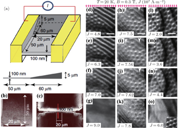
Very recently, Yu et al. reported the real-space observation of a biskyrmion, as defined by a molecular form of two bound skyrmions with the total topological charge of 2, realized under magnetic field applied normal to a thin plate of a bilayered manganite with centrosymmetric structure. They have observed a distorted-triangle lattice of biskyrmion crystal using a Lorentz transmission electron microscopy (TEM), which is composed of two bound skyrmions with oppositely swirling spins (magnetic helicities). Furthermore, they demonstrated that these biskyrmions could be electrically driven with several orders of magnitude lower current density (< 108 A/m2) than that for the conventional FM domain walls.[19] The detailed structure of the microdevice can be seen in Fig.
 | Fig. 5. Observation of stripes and biskyrmions under current excitations in a microdevice based on a bilayered manganites La2−2xSr1+2xMn2O7 with x = 0.315. (a) Schematic of the microdevice. (b), (c) Scanning-ion-microscopy images of the plane and cross-section views of the microdevice. (d)–(o) Lorentz TEM images of stripes and biskyrmions obtained under current excitations. Changes in magnetic configurations with increasing current J (in unit of 107 A/m2), obtained under a magnetic field of 0.3 T applied normal to the (001)-plane device plate at 20 K. (d)–(g) A mixed state of screws and biskyrmions at J = 4.8 × 10⁷ A/m2–9.0 × 107 A/m2. (h)–(k) A mixed state at finely tuned J (7.5 × 10⁷ A/m2–7.8 × 107 A/m2) and (l)–(o) a single-phase biskyrmion lattice state at J = 2.0 × 10⁷ A/m2–6.0 × 107 A/m2. Red arrows indicate the current direction. The insert at the right bottom corner shows the biskyrmion lattice without current excitation. Scale bars in panels (d), (h), and (l) correspond to 500 nm. Reprinted with permission from Ref. [19]. Copyright 2014, Nature Publishing Group. |
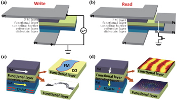
According to the above discussion, Joule heat from high threshold current density during the STT process is one of the major sources of the energy consumption in spintronic devices. Based on the above controls of magnetic phase boundaries, DWs or topological spin structures such as skyrmions, manganites may be integrated with a capacitor-based structure so that the write-in and read-out process will not induce a large charge current across the whole devices. Wang et al. discovered that the estimated instantaneous threshold current density at the tip/film interface for DW motion is even ∼ 3–4 orders of magnitude lower than that in transition metals, and there is no direct current flows through the circuit.[59] This capacitor-based geometry provides us a new technique for nanoscale control of spin structures with ultralow energy consumption. Therefore, we propose a prototype concept of information storage unit (magnetic phase boundaries, DWs or topological spin structures such as skyrmions in manganites) integrated in a capacitor-based multilayer structure as shown in Fig.
 | Fig. 6. Spintronic devices ingredient in capacitor-based multilayer structures. (a) Schematic diagram of writing process of the spintronic device. The writing process occurs with the changing of spin state in functional layer, which is correlated to the motions of phase boundaries, domain walls, and skyrmions driven by STT during charging and discharging processes in the capacitor. (b) Schematic diagram of reading process of the spintronic device. TMR of functional layer/tunneling barrier/reference layer is recorded to read ‘0’ (large TMR) and ‘1’ (small TMR) digital bits. (c) and (d) Schematics of multilayer structures ingredient in all kinds of spintronic devices based on the motion of phase boundaries (c), domain walls with in-plane (c), and out-of-plane (d) anisotropy, and skyrmions (d). FM layer is used to polarize electrons during writing process. Functional layer is composed of manganites thin film with different spin states. The magnetization of reference layer is determined by the bottom FE/AFM layer, which also serves as dielectric layer of the capacitor. The magnetic anisotropy of FM, reference, and FE/AFM layers could be either in-plane or out-of-plane, which is determined by spin states in manganites. In panel (c), the figure of domain wall with in-plane anisotropy reprinted with permission from Ref. [85]. Copyright 2014, IOP Publishing Ltd. In panel (d), the figure of skyrmion reprinted with permission from Ref. [18]. Copyright 2013, Nature Publishing Group. |
The write-in process is correlated with the motions of the so-called functional layers (e.g. phase boundaries, domain walls, or skymions in manganites), which can be driven by STT when spin-polarized electrons go through the functional layer (with in-plane or out-of-plane anisotropy) during charging and discharging of the capacitor (Fig.
We reviewed the physical properties and dynamic controls of nanoscale spin structures (at phase boundaries, domain walls, as well as topological spin structures such as skyrmions) in manganites. Additionally, a new concept of spintronic device is proposed, which is based on the nanoscale modulation of those low-dimensional spin structures in manganites integrated in a capacitor-based spintronic devices. We hope this prototype concept could provide a new geometry for next-generation spintronic applications with low energy consumption.
| 1 | |
| 2 | |
| 3 | |
| 4 | |
| 5 | |
| 6 | |
| 7 | |
| 8 | |
| 9 | |
| 10 | |
| 11 | |
| 12 | |
| 13 | |
| 14 | |
| 15 | |
| 16 | |
| 17 | |
| 18 | |
| 19 | |
| 20 | |
| 21 | |
| 22 | |
| 23 | |
| 24 | |
| 25 | |
| 26 | |
| 27 | |
| 28 | |
| 29 | |
| 30 | |
| 31 | |
| 32 | |
| 33 | |
| 34 | |
| 35 | |
| 36 | |
| 37 | |
| 38 | |
| 39 | |
| 40 | |
| 41 | |
| 42 | |
| 43 | |
| 44 | |
| 45 | |
| 46 | |
| 47 | |
| 48 | |
| 49 | |
| 50 | |
| 51 | |
| 52 | |
| 53 | |
| 54 | |
| 55 | |
| 56 | |
| 57 | |
| 58 | |
| 59 | |
| 60 | |
| 61 | |
| 62 | |
| 63 | |
| 64 | |
| 65 | |
| 66 | |
| 67 | |
| 68 | |
| 69 | |
| 70 | |
| 71 | |
| 72 | |
| 73 | |
| 74 | |
| 75 | |
| 76 | |
| 77 | |
| 78 | |
| 79 | |
| 80 | |
| 81 | |
| 82 | |
| 83 | |
| 84 | |
| 85 |