Nanoscale control of low-dimensional spin structures in manganites

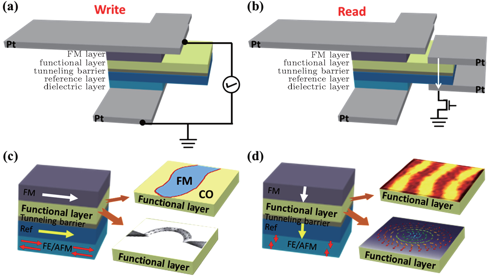
Spintronic devices ingredient in capacitor-based multilayer structures. (a) Schematic diagram of writing process of the spintronic device. The writing process occurs with the changing of spin state in functional layer, which is correlated to the motions of phase boundaries, domain walls, and skyrmions driven by STT during charging and discharging processes in the capacitor. (b) Schematic diagram of reading process of the spintronic device. TMR of functional layer/tunneling barrier/reference layer is recorded to read ‘0’ (large TMR) and ‘1’ (small TMR) digital bits. (c) and (d) Schematics of multilayer structures ingredient in all kinds of spintronic devices based on the motion of phase boundaries (c), domain walls with in-plane (c), and out-of-plane (d) anisotropy, and skyrmions (d). FM layer is used to polarize electrons during writing process. Functional layer is composed of manganites thin film with different spin states. The magnetization of reference layer is determined by the bottom FE/AFM layer, which also serves as dielectric layer of the capacitor. The magnetic anisotropy of FM, reference, and FE/AFM layers could be either in-plane or out-of-plane, which is determined by spin states in manganites. In panel (c), the figure of domain wall with in-plane anisotropy reprinted with permission from Ref. [