

Heterogeneous integration of GaAs pHEMT and Si CMOS on the same chip
[Wu Li-Shu†,  , Zhao Yan, Shen Hong-Chang, Zhang You-Tao, Chen Tang-Sheng]
, Zhao Yan, Shen Hong-Chang, Zhang You-Tao, Chen Tang-Sheng]
|
|


† Corresponding author. E-mail:
In this work, we demonstrate the technology of wafer-scale transistor-level heterogeneous integration of GaAs pseudomorphic high electron mobility transistors (pHEMTs) and Si complementary metal–oxide semiconductor (CMOS) on the same Silicon substrate. GaAs pHEMTs are vertical stacked at the top of the Si CMOS wafer using a wafer bonding technique, and the best alignment accuracy of 5 μm is obtained. As a circuit example, a wide band GaAs digital controlled switch is fabricated, which features the technologies of a digital control circuit in Si CMOS and a switch circuit in GaAs pHEMT, 15% smaller than the area of normal GaAs and Si CMOS circuits.
A cmompound semiconductor device has some special advantages like high-speed, high-voltage, while Si CMOS has shown unsurpassed levels of scaling and circuit complexity. It will be advantageous for many applications if we can integrate both Si CMOS and compound semiconductor transistors into one circuit or system.[1–3] In general, separate circuits or circuit blocks with dissimilar materials can be interconnected by gold wire bonding or flip chip technology if the number of interconnections is small and the interconnect signal speed is not extremely high. However, the gold wire bonding technology will bring a large coupling effect between the bonded gold wires, and more parasitic effects are introduced on the longer wire, these coupling effects and parasitic effects become more serious with the increase of the operating frequency of the circuit. The flip chip technology is affected by the precision of the equipment: the spacing between the solder joints is generally above 100 μm, which directly restricts the integration of density and flexibility. In a higher-density integrated circuit, there are hundreds and thousands of interconnects, which will lead to a sharp increase of the chip area and parasitic parameters by flip chip technology, as well as a sharp decline of the product yield. While for chips that are required to possess higher performances, smaller size and minimum interconnect length, the technology of transistor-level integration where heterogeneous interconnects are comparable in length and density to standard semiconductor ones, is required.[4] This seamless combination of both compound semiconductor and Si CMOS would provide circuit designers with the flexibility to choose the best junction for each function between the two technologies.[5] Thus, a new kind of high-performance or multiple-function IC would be achieved which could not be made only by one of the technologies.
There are several ways to achieve the transistor-level heterogeneous integration of compound semiconductors and Si CMOS. One is by performing metamorphic epitaxial growth of two different materials on the same substrate. The other is by transferring the epitaxial layer of compound semiconductors to the Si substrate, and then processing the III–V devices.[6,7]
In this paper, we present an innovative approach to achieving wafer-scale transistor-level heterogeneous integration of GaAs pHEMT and Si CMOS based on the epitaxial layer transfer technique. The GaAs pHEMTs are first processed and then transferred from the original GaAs substrate to the top of a ready-made Si CMOS wafer. A hybrid digital controlled switch is fabricated as a circuit demonstrator, which shows the potential to integrate compound semiconductors and Si CMOS on the same chip to take advantage of the two different material systems.
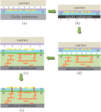
Figure
 | Fig. 1. The schematic representation of the process flow chart. |
The GaAs pHEMT wafer is bonded to a temporary handle wafer with the device-side contacting to the carrier as shown in Fig.
There are two essential technical challenges in our wafer-scale transistor-level heterogeneous integration technology. One is to achieve a crack- and crinkle-free patterned GaAs pHEMT epitaxial layer after the substrate removal, and it is more difficult when the wafer size is large. Concerning this problem, we can make efforts of the temporary bonding process to ensure that the bonding layer is flat and void-free. What is more important is that the thermal expansion coefficient of the handle wafer must well match with the GaAs substrate. It will minimize the wafer bow after temporary bonding. The other challenge is to achieve a precise alignment accuracy of the permanent bonding in order to obtain transistor-level integration of GaAs pHEMT and Si CMOS. In this work, the GaAs pHEMT layers with the handle wafer and Si CMOS wafer with alignment marks are spin-coated with BCB. Then the BCB is soft-baked and partially cured at 190 °C. The two wafers are aligned in the SUSS BA6 bond aligner and bonded in SUSS SB6 wafer bonder at 250 °C. The partially cured BCB layer does not reflow during bonding, thereby minimizing the influence of inhomogeneities in BCB reflow under compression and shear forces at the bonding interface. The best alignment accuracy we obtained using this method is about 5 μm and could be further improved by several approaches.
Considering the fact that the BCB is sandwiched between GaAs pHEMTs layers and Si CMOS, besides the BCB having low thermal conductivity, we should evaluate the different thickness values of BCB which affect the performances of GaAs pHEMTs. A total of four groups of wafer bonding experiments are performed, the BCB thickness is uniform after wafer bonding, neither crack nor void-free bond with the BCB is achieved.
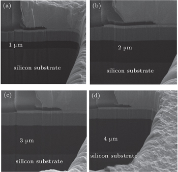
The BCB is spun onto Si CMOS wafers with thickness values ranging from 1 μm to 4 μm, respectively. When the bonding process is completed, the BCB is checked up through a focused ion beam (FIB) as shown in Fig.
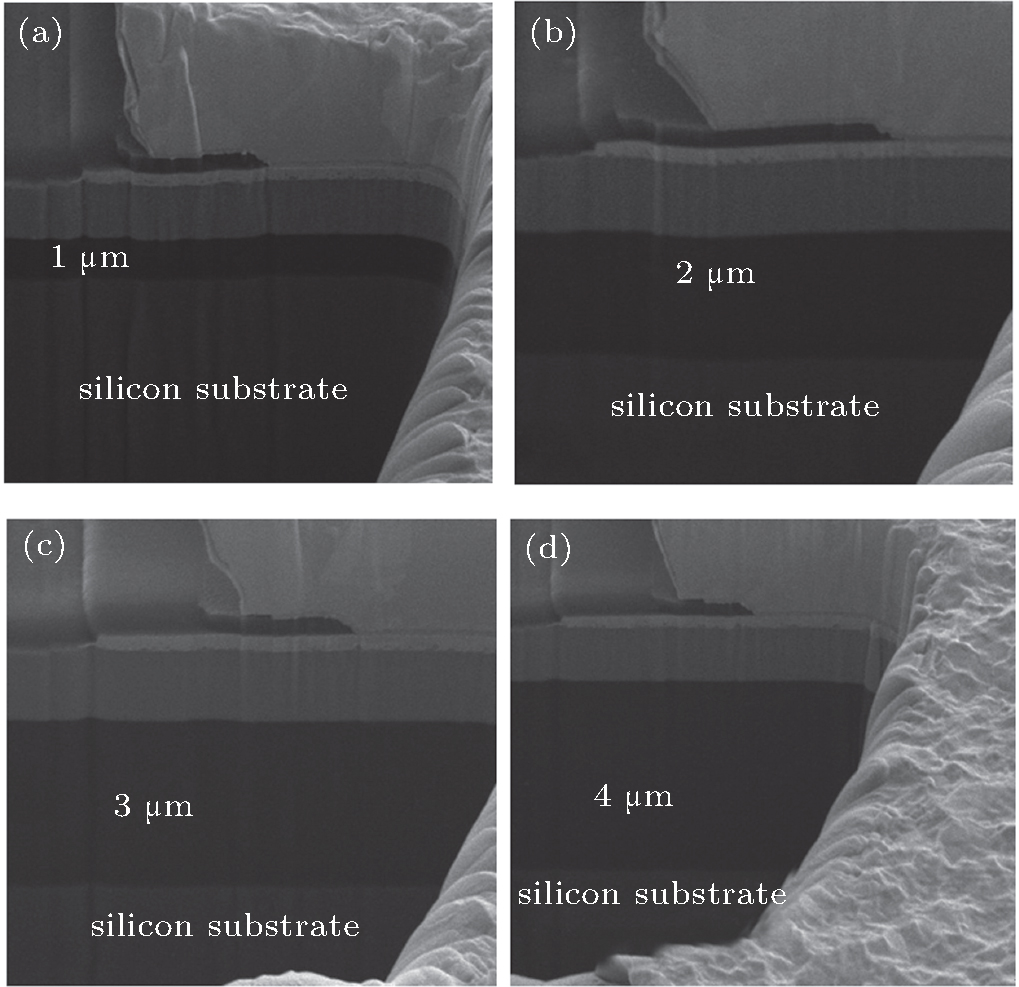 | Fig. 2. Cross-sectional views of fabricated GaAs pHEMTs on Si CMOS, with (a) 1 μm-BCB, (b) 2 μm-BCB, (c) 3 μm-BCB, and (d) 4 μm-BCB. |
Then IV measurements of GaAs pHEMT are carried out on a semi-automatic wafer prober. Figure
 | Fig. 3. I–V characteristic curves of standard GaAs pHEMT and transferred GaAs pHEMT with (a) 1-μm BCB, (b) 2-μm BCB, (c) 3-μm BCB, and (d) 4-μm BCB, respectively. |
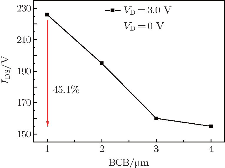 | Fig. 4. Relationship between IDS and thickness of BCB at VD = 3.0 V and VG = 0.0 V. |
The main reason is because of the low thermal conductivity of the BCB (0.29 W/mK at room temperature);[8] the improvement in thermal resistance could be gained by the BCB between the GaAs pHEMT device and the silicon substrate. While the thickness of BCB is less than 1um, the DC characteristic of GaAs pHEMT will be unaffected.
Thermal effects and BCB have a large influence on post-bond accuracy. The mismatch between the InP- (4.6 ppm·K−1) and Si-(2.6 ppm·K−1) substrate thermal expansion coefficients during the wafer-bonding induces an isotropic expansion of the InP layout at the top of the CMOS wafer of ∼ (350 ± 10) ppm, which is precompensated for in the layout.
The front-side alignment of Si CMOS with digitalized image can be used by an optical microscope, with this approach, the carrier wafer must be transparent. The wafer-to-wafer alignment accuracy is measured with infrared microscopy (silicon wafers are transparent to infrared light) using the alignment keys at the left and right wafer edges.[9] However, it is difficult to inspect the post-bonding alignment accuracy with IR since the alignment marks on both wafers are not on the same focal plane.
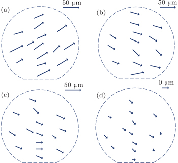
After the BCB bonding is performed, the wafer-to-wafer alignment accuracy is measured and compared with the pre-bond wafer-to-wafer alignment accuracy.[10] The difference between pre-bond and post-bond alignment accuracy represents the shift of the wafers with respect to each other in the wafer bonding process, i.e., the bonding-induced misalignment. A total of four wafer bonding experiments are performed, and the results are shown in Fig.
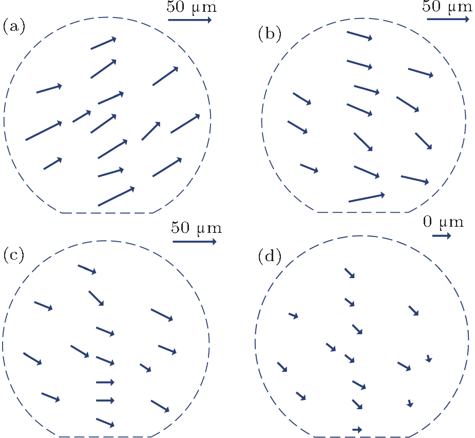 | Fig. 5. Displacement vector fields for initial bond experiments at partially cured temperatures of 160 °C (a), 170 °C (b), 180 °C (c), and 190 °C (d), each for 1 h, respectively. |
Based on a partially cured temperature of 190 °C, the mean value of the wafer shifts with respect to each other in the wafer bonding process is 5um at the right and left alignment keys as shown in Fig.
 | Fig. 6. Micrographs of misalignment of GaAs and Si CMOS. |
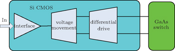
To demonstrate the capabilities of the GaAs-on-CMOS integration, an integrated digital single pole double throw switch is presented. The main structure of the integrated switch circuit is shown in Fig.
 | Fig. 7. Structure diagram of GaAs numerical controlled single pole double throw switch circuit. |
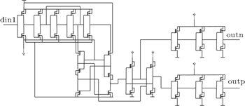
The CMOS circuit is a silicon drive circuit,[11] which acts as driving the single pole double throw switch circuit, and transferring external TTL/CMOS voltage into 0 V/(−5) V negative voltage logic of GaAs pHEMT switch, to make the switch to work normally under the control of an external signal. The CMOS drive circuit consists of three parts as shown in Fig.
 | Fig. 8. Topology of Si CMOS drive circuit. |
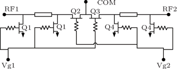
GaAs pHEMT single pole double throw switch circuit adopts a series-parallel structure, because of the demand of isolation and process, the topology of one series and two parallel is designed as shown in Fig.
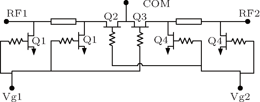 | Fig. 9. Topology of GaAs single pole double throw switch circuit. |
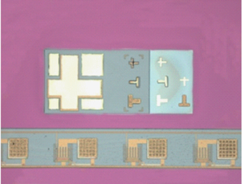
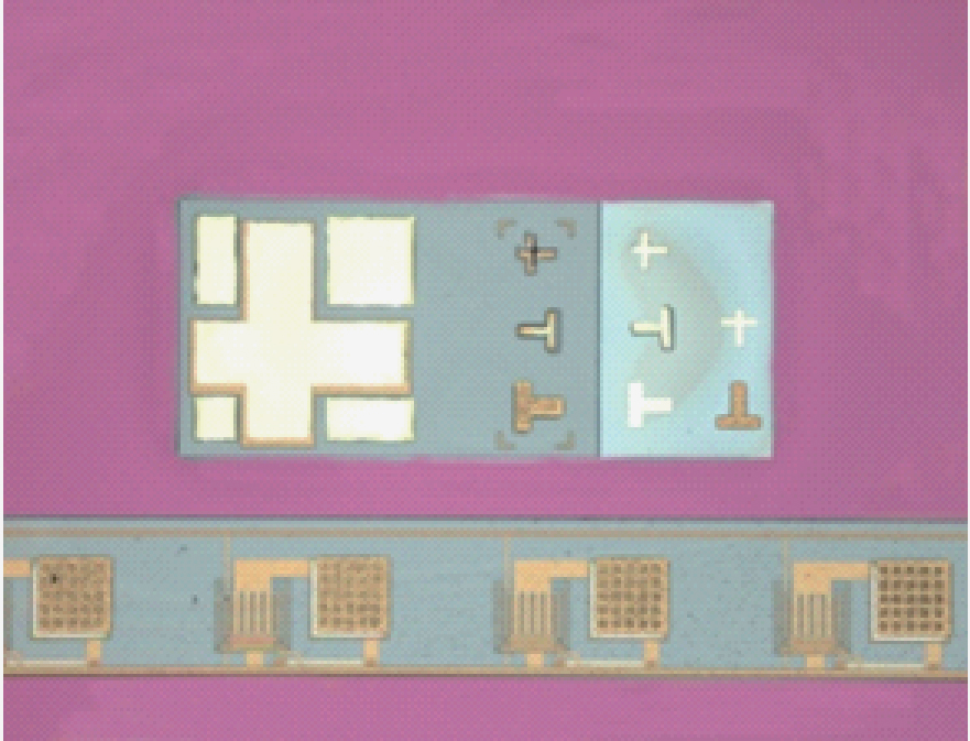
Figure
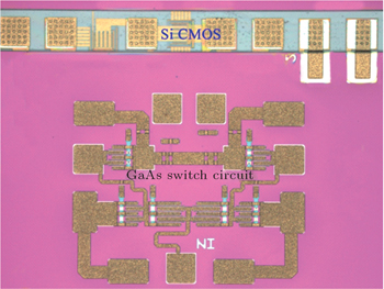
 | Fig. 10. The chip micrograph of the entire hetero-integrated circuit. |
Figure
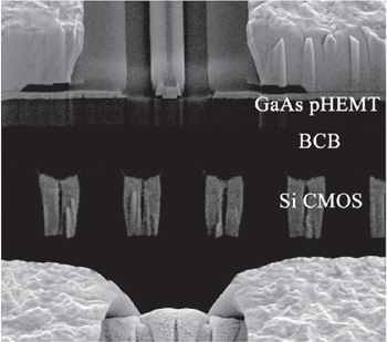
 | Fig. 11. Focused ion beam (FIB) cross-section of the chip area. |
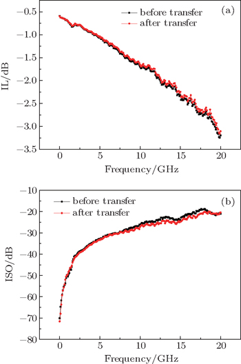
To investigate the influence of the heterogeneous integration on the Si CMOS circuits (the GaAs switch circuits are unaffected by the heterogeneous integration process), the performances of the GaAs test devices, of which some have gone through the normal process only and the others went through the heterogeneous integration are compared, and the results are shown in Fig.
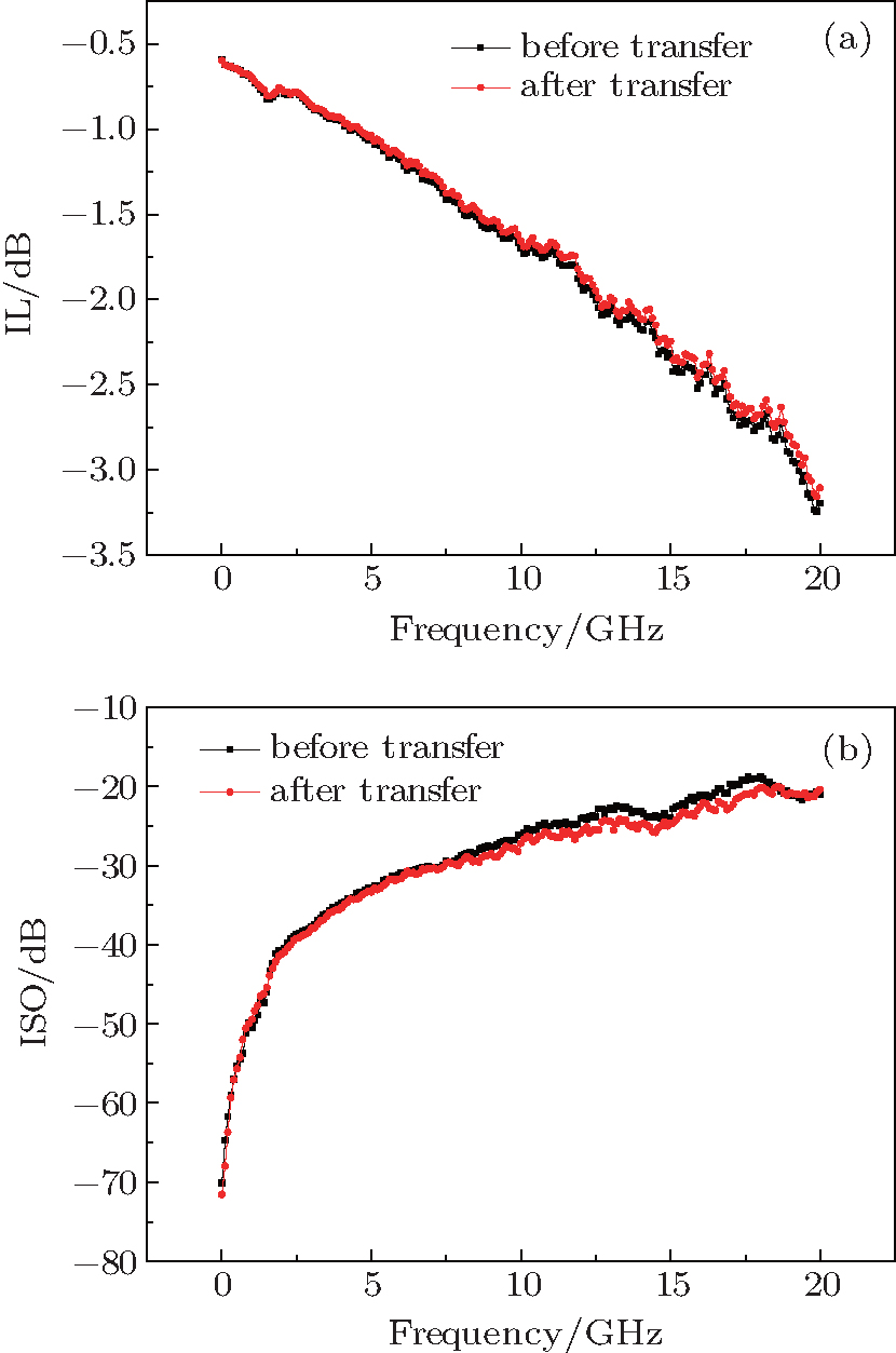 | Fig. 12. Comparisons of insertion loss and isolation between before and after transfer. |
We demonstrate the technology of wafer-scale transistor-level heterogeneous integration of GaAs pHEMTs and Si CMOS on the same Silicon substrate. The GaAs pHEMTs are vertically stacked at the top of the Si CMOS wafer by using the wafer bonding technique, and the best alignment accuracy of 5 μm is obtained. With this technology, both III–V device speed and CMOS low power dissipation can be simultaneously obtained for one chip. As a circuit example, a wide-band digitally controlled switch is fabricated, which features the technology of the digital control circuit in Si CMOS and the switch circuit in GaAs pHEMT, and the GaAs switch circuits are unaffected by the heterogeneous integration process. It demonstrates an overall performance, which could not be achieved only by either of the employed processes. Such a seamless three-dimensional integration scheme is able to unlock synergies from complementary semiconductor technologies without tradeoffs to achieve performance levels far beyond those of their individual roadmaps.
| 1 | |
| 2 | |
| 3 | |
| 4 | |
| 5 | |
| 6 | |
| 7 | |
| 8 | |
| 9 | |
| 10 | |
| 11 |