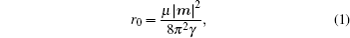
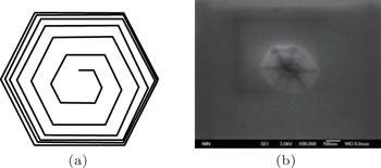
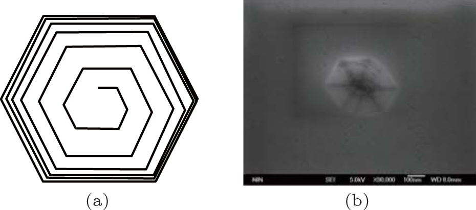
1. IntroductionIn 1949, Frank[1–3] proposed his famous theory of dislocation mediated crystal growth that has been widely used for interoperating the crystal growth from vapor phase onto a foreign substrate. It states that the screw dislocation will cause a surface displacement equal to the component of the Burgers vector normal to the surface in order to achieve a balance between the surface energy and dislocation strain energy, which is manifested in step line running outwards from the termination of dislocation. Perpetual growth can continue on these steps, making two-dimensional nucleation unnecessary. Two years later in 1951, Frank[4] and Burton et al.[5] further pointed out that this step growth around the screw dislocation core would result in an inverted pyramid pit on the free surface. The step due to the dislocation will rapidly wind itself up into a spiral centered on the dislocation, like the shape of a spiral staircase. When the curvature at the center reaches the critical value 1/r0, at which the accelerating rate of the curvature falls to zero; the whole spiral will then rotate steadily with stationary shape as schematically shown in Fig. 1(a).
By balancing the elastic dislocation strain energy against the energy of the resulting free surfaces, Frank showed that the equilibrium curvature radius at the dislocation center is[4,6]
where
b is the component of the Burgers vector that is parallel to the dislocation line,
μ is the rigidity modulus, and
γ is the surface free energy. Assuming that the surface energy is independent of orientation for simplification, the radius
r and the depth
h of the spiral steps satisfy the relationship in an approximation
[4]

The slope 1/4 occurs at r/r0 = 10.5. The radius of the resulting surface pit can be estimated to be 10r0 accordingly. Frank also calculated the elastic strain for edge dislocation, however, the surface depression would be of finite (if not zero) depth and volume. Hence the pit formation requirement is that the dislocation line must be parallel to the Burgers vector as in the case of screw dislocation.
Evidence for this novel mechanism was soon found, with some of the first observations of spiral growth on the surface of SiC.[7,8] Early work about c-plane GaN epitaxial film grown by metal organic chemical vapor deposition (MOCVD) has also widely reported this kind of surface pit caused by surface termination of screw dislocation (b = ± [0001]).[9–16] Figure 1(b) is the scanning microscopy electron (SEM) image of a hexagonal pit we have observed on c-plane GaN surface. The spiral steps on the pit facets could be seen. Recently, in our work[17] on a-plane GaN, both pure screw dislocation  and partial dislocation (PD) (Frank–Schockley type
  and Shockley type
  have been found to cause triangular shaped pits on the surface, due to the fact that the Burgers vector of PD has the component in the direction parallel to the dislocation line. A pit resulting from PD possesses much smaller size than the pit produced by pure screw dislocation for the smaller screw component.
Nevertheless, there remains an important discrepancy: the size of the pit observed in experiment is not consistent with that obtained from Frank’s theory. For c plane, given γ of 2.0 J/m2, μ of 67 GPa and the c-axis lattice parameter 0.516 nm, the calculated equilibrium curvature radius r0 is 0.11 nm, and the pit size is approximately 1.1 nm. However, in most of the experiments, the pits are of tens of nanometers[10–12,15] up to hundreds of nanometers.[9,13,14,16] Researchers have tried to explain it. Early work suggested that the surface steps in the sapphire substrate would affect the pit formation mechanism,[11] however, nowadays, GaN epitaxial films are grown by a two-step procedure, which introduces a buffer layer in-between the foreign substrate and the as-grown film.[18,19] Some of the researchers believed that the impurity segregation to the dislocation core may contribute to the pit formation process.[9,10,16,20] When the concentration of the impurity atoms increases to a certain degree, it may slow down or inhibit the crystal growth in the surrounding area, which initiates the pit formation,[10] and indeed most of the reported surface pits are found in InGaN samples[10,14–16] or samples doped with Si[13] and Mg.[9] However, pits on samples without intentional doping are still observed.[12] We have also found pit formations on undoped c-plane GaN grown under low V/III ratio. Therefore, the impurity atom is not the necessary condition for the pit formation.
It should be noticed that Frank’s model is only applicable in the thermodynamic equilibrium condition. Although MOCVD has long been assumed to be a near equilibrium process, nitrides are different in that the temperature employed is high and barriers such as NH3 dissociation are functioning.[21] Hence in practice nitride MOCVD is a non-equilibrium process,[21,22] and heteroepitaxy of GaN inherently consists of numerous atomistic processes governed by competitions between kinetics and thermodynamics. We believe that Frank’s theory would still be valid in that thermodynamic equilibrium will be in effect in the local dislocation core area, but in the large surrounding area, facet formation governed by the kinetic process will enlarge the pit.
2. Validity of Frank’s model under local equilibrium assumptionGlansdorff and Prigogine in their famous theory[23] of dissipation system believed that there is no impassable gap separating the equilibrium state and non-equilibrium state. They emphasized the assumption of local thermodynamic equilibrium that there exists within each small mass element of the medium a state of local equilibrium for which the local entropy is the same function of the local macroscopic variables as at equilibrium state. The assumption of local equilibrium is not in contradiction with the fact that the system as a whole is out of equilibrium. As a simple example taken by Glansdorff and Prigogine, expansion of a gas in a pipe corresponds to a non-equilibrium process, however, at each point the relation among temperature, pressure and density is still expressed by the same law, e.g., pv = RT, as that for equilibrium state. In other words, the local state is completely described by an equation of state independent of the gradients. Such situations occur in many problems of macroscopic physics. Considering the process of reaching local equilibrium state, enough collision processes are needed in the system, so the assumption of local equilibrium certainly does not hold true in highly rarefied gases when collisions become too infrequent, or for interacting fermions at very low temperature. Since for nitride MOCVD the atomic transport processes to get ordering can be described by linear laws,[21] and the deposition is not a too-fast chemical reaction, so the local equilibrium assumption can be applied.
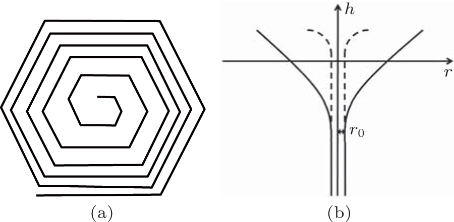
Under this assumption, Frank’s model is valid only in a small range of area, where thermodynamic equilibrium can be achieved. If this local range of area is large enough so that the spiral center and edge are in the same equilibrium state, when the curvature at the center reaches the critical value 1/r0, the whole spiral will then rotate steadily with the stationary shape till the end of growth. The pit size would exactly follow Frank’s model. The dashed line in Fig. 2(b) is the h ∼ r relationship that is constructed according to Eq. (2) in the original paper of Frank.[4] Although Frank’s calculation is based on an isotropic system, GaN has a hexagonal crystal structure and therefore the basal plane (i.e., 0001), and all planes perpendicular to it, are elastic symmetry planes, which exhibit pseudo-elastic isotropy. As a result, the calculated result could be used.
However, if the local equilibrium range is too small for the spiral center and edge to keep in the same equilibrium state, when the curvature at the center of the dislocation core reaches the critical value 1/r0, at the edge of the spiral, the accelerating rate of the curvature may not fall to zero. Thus the pit cannot reach a stationary shape and will keep enlarging. Figure 2(a) illustrates this mechanism as a comparison with the scenario in Fig. 1(a). The elastic energy associated with the dislocation will not come into effect at the edge of the pit, so equation (2) is invalid. Faceting of the pit is only dominated by the ultimate driving force, i.e., surface energy, and can be empirically determined through the kinetic Wulff construction, which extends the procedure of Wulff plot to non-equilibrium growth, based on the minimization of total surface energy under equilibrium condition.[22] The exposed facets would be the {1011} planes, which are about 60° with respect to the c-plane. The solid line in Fig. 2(b) is the schematic pit profile in practice when the same equilibrium state cannot be achieved between the center and the edge of the screw dislocation spiral.
As a result, the more the system approaches the equilibrium growth, the larger the range for keeping the same local equilibrium state is and the smaller the surface pit in size. If the kinetic process is too vigorous or too slow to reach a balance, the local equilibrium range is small, and the resulting surface pit is large. Since the kinetic process in MOCVD contains many independent parameters, the valid range for keeping the same local equilibrium state and the resulting pit size are determined by growth conditions, and currently can only be qualitatively analyzed based on experimental observations.
3. ExperimentsGrowth of GaN epitaxial film was achieved using a cold-wall showerhead MOCVD system, using hydrogen as the carrier gas and triethylgallium (TEG) and ammonia (NH3) as source compounds. The reactor pressure was 5333 Pa. The c-plane (0001) GaN was grown on c-plane sapphire substrate. A low-temperature (LT) GaN buffer layer was grown at 450 °C first, and followed by a high-temperature (HT) GaN layer. Since the kinetic process is highly determined by the growth temperature and V/III ratio, a set of samples was prepared with the temperature varying in a range of 865 °C–965 °C, the V/III atom ratio in a range of 1940–3160. Each time, only one growth parameter was changed while the others were kept unchanged. The thickness is in a range of 1 m–1.5 m.
An atomic force microscope (AFM) was used to characterize the sample surface morphology. The pit size and height were measured by the section profile. AFM could provide a more accurate density value than SEM, because not all the pits are in the same focal plane of SEM, and some of the small pits cannot be discerned. X-ray diffraction (XRD) was used to characterize the structural properties for a comparison. High-resolution scanning electron microscopy (HRSEM) was used to observe the local surface characteristics. The sample surface was first cleansed by plasma to remove the carbon adhesion. Transmission electron microscope (TEM) analysis was used to study the structure origin of the surface pits. The TEM specimens were prepared by a focused ion beam (FIB).
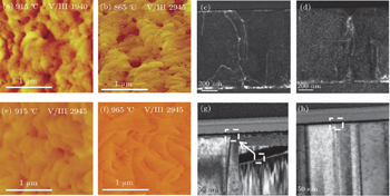
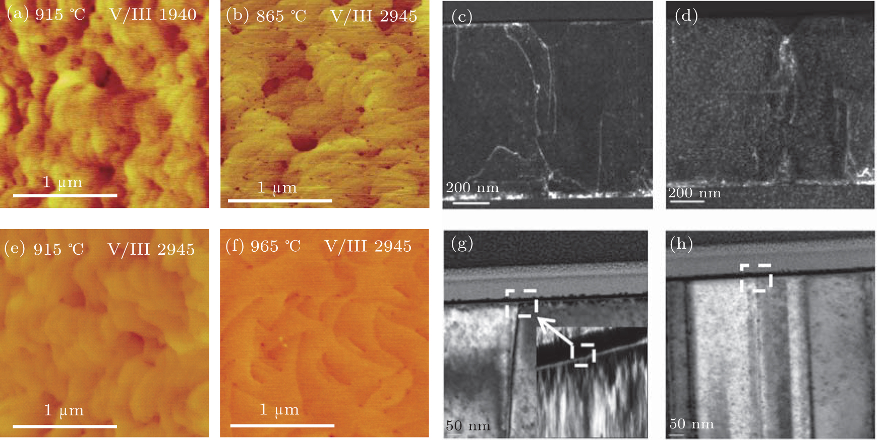
4. Experimental resultsSurface pits are observed to be connected with screw dislocations, however, their appearances are highly influenced by growth conditions. Low V/III atom ratio or low temperature would promote these pits. Figure 3(a) is the 2 μm×2 μm AFM image of the c-plane GaN morphology grown under low V/III atom ratio but high temperature (V/III atom ratio of 1940 and temperature of 915 °C, Sample No. G). Figure 3(b) is the 2 μm×2 μm AFM image of the c-plane GaN morphology grown under high V/III atom ratio but low temperature (V/III atom ratio of 2945 and temperature of 865 °C, Sample No. C). Surface pits appear as scattering dark spots, located at the intersections of surface steps. The pit densities for both samples are close to 109 cm−2. Among the pit sizes, some are close to 200 nm, while the majority are below 10 nm. These pits are identified with screw type of dislocation. According to the invisible criteria,[24] perfect dislocation is invisible when g · b = 0, where b is the Burgers vector. When g = 1120, the visible defects are perfect edge dislocations  and mixed-type dislocations (b = ± ⟨1123⟩,
  , and
, and  ). When g = 0002, the visible defects are perfect screw dislocations with b = ± [0001] and mixed-type dislocations
  . Since the dislocation line that is connected with the apex of the pit only appears under g = 0002 as comparatively shown in Figs. 3(c) and 3(d), it is of pure screw dislocation. The bright blurred area under the pit in Fig. 3(d) is not defect contrast, because its shape is not sharp nor regular. The bright blinking spots are the small crystal grains, which are due to the sample damage caused in the preparation process.
Surface pits will become less distinguished under high V/III atom ratio and high temperature simultaneously. Figure 3(e) shows a 2 μm×2 μm AFM image of the sample grown under a V/III atom ratio of 2945 and temperature of 915 °C (Sample No. B). The pit density is about 108 cm−2. The pit becomes indistinctive, which indicates that its size is below the AFM resolution (about 2nm, given the resolution of 1024×1024 in a 2 μm×2 μm image). In the cross-sectional TEM image, a pit is vaguely observed under enlarged view as shown in the inset of Fig. 3(g), and its end still shows the connection with a pure screw dislocation line since the dislocation line appears in the image with g = 0002 in Fig. 3(g) and disappears in the image with g = 1120 in Fig. 3(h). It should be noted that further increasing the temperature will slightly enlarge the pit size. Figure 3(f) shows the AFM image of the sample grown under a V/III atom ratio of 2945 and temperature of 965 °C (Sample No. A).
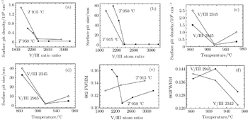
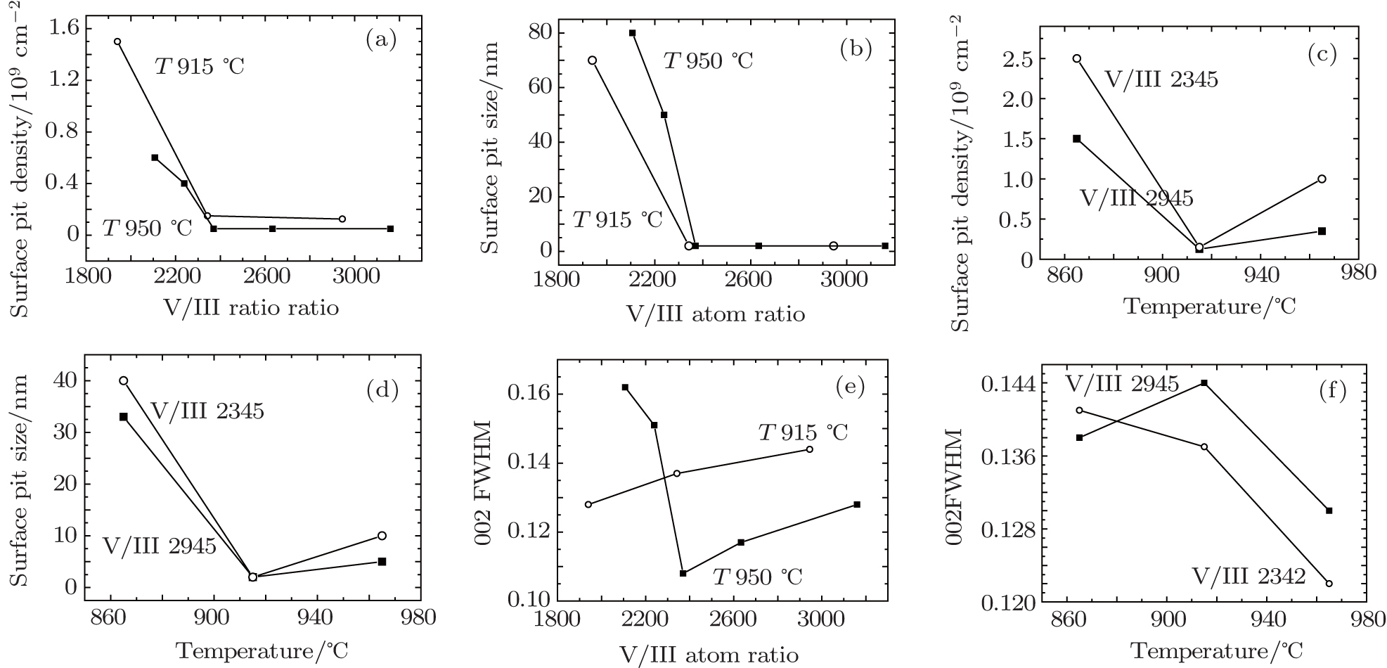
Summarized in Table 1 is the sample information about the surface pit density and size under different growth conditions. With increasing growth V/III atom ratio, the surface pit density and size decrease monotonically as plotted in Figs. 4(a) and 4(b). With increasing temperature, the pit density and size first decrease significantly and then slightly increase as shown in Figs. 4(c) and 4(d). There are two sets of samples that show similar trends, which affirms the observed phenomenon. The variation of surface pit density with V/III atom ratio is more significant under lower temperature, and the variation of pit density with temperature is more significant under lower V/III atom ratio.
Table 1.
Table 1.
 Table 1. Variations of surface pit density and size with growth condition of c-plane GaN. .
| Samples |
V/III |
Temperature/°C |
Surface pit density/cm−2 |
Average pit size/nm |
(0002) FWHM/(°) |
| A |
2945 |
965 |
3.50×10⁸ |
5 |
0.130 |
| B |
2945 |
915 |
1.25×10⁸ |
≦ 2 |
0.144 |
| C |
2945 |
865 |
1.50×10⁹ |
33 |
0.138 |
| D |
2342 |
965 |
1.00×10⁹ |
10 |
0.122 |
| E |
2342 |
915 |
1.50×10⁸ |
≦ 2 |
0.137 |
| F |
2342 |
865 |
2.50×10⁹ |
40 |
0.141 |
| G |
1940 |
915 |
1.50×10⁹ |
70 |
0.128 |
| H |
3160 |
950 |
5.00×10⁷ |
≦ 2 |
0.128 |
| I |
2633 |
950 |
5.00×10⁷ |
≦ 2 |
0.117 |
| J |
2370 |
950 |
5.00×10⁷ |
≦ 2 |
0.108 |
| K |
2239 |
950 |
4.00×10⁸ |
50 |
0.151 |
| L |
2107 |
950 |
6.00×10⁸ |
80 |
0.162 |
| Table 1. Variations of surface pit density and size with growth condition of c-plane GaN. . |
Although the density of surface pits is in the same order as the density of screw dislocations as generally reported,[25] it does not show correlation with the FWHM of (0002) plane ω-scan in XRD, which is often used to describe the screw dislocation density.[26] Samples G and H possess the same FWHM, but their surface pit densities are completely different. The (0002) FWHM increases with increasing V/III atom ratio under 915 °C as shown in Fig. 4(e), which is opposite to the variation trend for the surface pit density, and the variation of the FWHM with temperature does not show slight increase with further increasing temperature as shown in Fig. 4(f). There are two reasons: first, not all the dislocations propagate to the surface. It can be seen in Fig. 3(c) that some of the dislocations bend near the interface of substrate/epitaxial-layer; second, the screw dislocation density may be of high level, but the resulting pits may be too small in size to be observed, and hence the measured pit density is of low level.
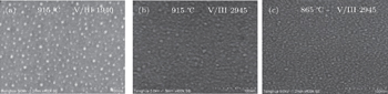
The surface kinetic equilibration process can be indirectly observed through observing the surface distribution of Ga droplets by HRSEM. Ga atoms are allowed to impinge on the substrate in the absence of nitrogen impinging on the surface. A balance between impinging and desorbing Ga flux will establish an equilibrium Ga coverage at the surface independent of deposition time. If the impinging Ga flux exceeds the desorbing flux, Ga accumulation takes place, eventually leading to the formation of droplets at the top of the adlayer. The thin equilibrium Ga adlayer and Ga droplets at the top of it have generally been observed using in-situ monitoring measurements.[21,27] After growth, the Ga droplets can still be seen under high magnification in HRSEM. Figure 5 shows the high-magnification images of the samples grown under (a) a V/III atom ratio of 1940 and temperature of 915 °C (Sample G), (b) a V/III atom ratio of 2945 and temperature of 915 °C (Sample B), and (c) a V/III ratio of 2945 and temperature of 865 °C (Sample C). For the sample grown under relative low V/III atom ratio, the Ga droplets are more scattered and significant. It even gives a good electron reflection without charge storage effect, which will darken the SEM image. The average diameter of the Ga droplets is 8nm, and the average interval is 15 nm. With the same temperature, the high V/III atom ratio sample shows a tight distribution of Ga droplets, with an average interval of 2 nm. The aggregation of the droplets is not that significant. The average diameter of the Ga droplets is about 5 nm. Further reducing the temperature, the Ga droplets become a little more undistinguished but tighter, with an average diameter of 3 nm and interval of 1nm. It should be pointed out that neither the absolute value of the Ga droplet interval nor diameter can be directly used to describe the local equilibrium range, because the Ga droplet is just a result of the atom aggregation movement during growth, and can be only used as a hint to observe the status of equilibrium between absorption and desorption, as well as surface diffusion.
5. Accordance with the modelIt can be seen from the experimental results that the surface pit appearance is highly dependent on the growth conditions, which indicates that although screw component dislocation will cause a pit on the surface, the size of the pit is determined not only by the interplay between dislocation strain and surface energy, but also by the kinetic process of reaction atoms on the as-grown surface. Dislocation is just an inductive factor. The kinetic process must be taken into account. This is like a man’s stature is determined by the genetic factor as well as the acquired nutrition and exercise.
The GaN MOCVD kinetic process mainly involves the precursor adsorption and decomposition, Ga and N2 desorption, and surface diffusion, and growth is complex in that these processes take place simultaneously at many levels. Several factors, such as the precursor flux, the gas-phase diffusion rate, the sticking coefficient, the number of available surface sites, and the precursor decomposition rate, contribute to the concentration of active growth species on the surface. For simplicity, the kinetic model is generally described as a balance between adsorption and desorption.[21] A near equilibrium growth implies that the ratio between input fluxes, FN/FGa matches the ratio between the desorption fluxes, kN/kGa. In c-plane GaN growth, kN/kGa depends exponentially on temperature,[28] so if the temperature is high, the choice of FN/FGa must be high enough to make the growth approach more to a near equilibrium growth. Figure 5(b) shows the local surface condition that most approaches to the equilibrium growth among our samples investigated. Although Ga droplets do not completely vanish, they are less distinguished and more uniform in a small range compared with the case in Fig. 5(a). It may not be a complete equilibrium process, but the local equilibrium range will be large enough to cover the pit formation area. In this case, the pit formation proceeds according to Frank’s model, which gives rise to a small pit size. The pit density is correspondingly at a low level since some of the pits are too small to be observed. In accordance with the experimental results, a high V/III atom ratio and high temperature simultaneously lead to indistinct surface pits as shown in Fig. 3(e).
Adversely, low V/III atom ratio but high temperature implies that FN/FGa < kN/kGa. This non-equilibrium process is manifested by the formation of Ga droplets as seen in Fig. 5(a). The aggregation of Ga atoms is significant, and the large Ga droplet interval indicates that the local non-uniformity is large, so the local equilibrium range is small. According to the pit formation model we proposed in Section 2, since Frank’s model is only valid in a small local mass of area where the same equilibrium states can be assumed, far from the dislocation core, the accelerating rate of the spiral curvature will not fall to zero, and the pit will keep enlarging. Faceting of the enlarged pit will be completely controlled by surface energy. As seen from the cross-section in Fig. 3(c), the pit is bounded by the {1011} plane, which possesses the minimum surface energy off the c-plane as can be determined from the kinetic Wulff plot.[22]
In a high V/III atom ratio but low temperature condition, although Ga droplets become less distinguished, the Ga diffusion length is shortened at a reduced temperature. The N diffusion length is invariably zero because of the high ionic bond character for Ga–N.[28] So comparing Fig. 5(b) with Fig. 5(c), it can be seen that the Ga droplets are smaller but closer to each other under low temperature. For growth, the surface diffusion length is an important factor contributing to the net incorporation rate of atoms into the crystal. The increased adatom diffusivity should aid in the growth of a more ordered lattice,[28] on the contrary, too low a temperature will give rise to a non-equilibrium growth. Atoms need more time to get ordered, so the local equilibrium range is small, and the surface pits are large and significant as shown in Fig. 3(b). However, if the temperature is too high, the Ga diffusion length will reduce because the increase of diffusion coefficient with temperature will be counterbalanced by the large Ga thermal desorption rate. So the experimental results show a slight increase of surface pit density under the highest temperature.
It should be pointed out that a near equilibrium growth does not necessarily mean an optimized crystal quality, because dislocation and surface pit density do not show strong correlation. The extent to which growth approaches equilibration affects the surface morphology significantly, but dislocation formation will also be influenced by other factors, such as the bending mechanism. It indicates that an optimized growth is a compromise and cannot satisfy all the desired material quality characters. So if one wants to get a smooth surface and low dislocation density at the same time, at least two layers are needed: one layer is for reducing dislocations and the other is for controlling the surface morphology, because even though theoretically the surface pits are caused by dislocations, the pit size will not be negligibly small if growth is very close to equilibrium.
6. ConclusionsFrank’s model about the dislocation mediated surface comes into effect in the local surface area of GaN where thermodynamic equilibrium state stays unchanged. The more the system approaches the equilibrium growth, the larger the range for keeping the same local equilibrium state is and the smaller the surface pit in size. If the kinetic process is too vigorous or too slow to reach a balance, the local equilibrium range will be too small for center and edge of the screw dislocation spiral to be kept in the same equilibrium state. When the curvature at the center of the dislocation core reaches the critical value 1/r0, at the edge of the spiral, the accelerating rate of the curvature may not fall to zero, so the pit cannot reach a stationary shape and will keep enlarging thus resulting in a large sized surface pit. Frank’s model could explain why screw component dislocation will cause a pit on the surface, but the pit size highly depends on the growth kinetic process.


 , Xue Xiao-Wei, Li Jiang-Jiang, Wang Xun, Xing Yan-Hui, Cui Bi-Feng, Zou De-Shu]