Xi Xiao-Wen, Chai Chang-Chun, Zhao Gang, Yang Yin-Tang, Yu Xin-Hai, Liu Yang. Damage effect and mechanism of the GaAs pseudomorphic high electron mobility transistor induced by the electromagnetic pulse. Chinese Physics B, 2016, 25(4): 048503
Permissions
Damage effect and mechanism of the GaAs pseudomorphic high electron mobility transistor induced by the electromagnetic pulse
Xi Xiao-Wen1, †, , Chai Chang-Chun1, Zhao Gang2, Yang Yin-Tang1, Yu Xin-Hai1, Liu Yang1
Key Laboratory of Ministry of Education for Wide Band-Gap Semiconductor Materials and Devices, School of Microelectronics, Xidian University, Xi’an 701107, China
Complicated Electromagnetic Environment Laboratory of China Academy of Engineering Physics, Institute of Applied Electronics, China Academy of Engineering Physics, Mianyang 621900, China
Project supported by the National Basic Research Program of China (Grant No. 2014CB339900), and the Open Fund of Key Laboratory of Complex Electromagnetic Environment Science and Technology, China Academy of Engineering Physics (CAEP) (Grant No. 2015-0214.XY.K).
Abstract
Abstract
The damage effect and mechanism of the electromagnetic pulse (EMP) on the GaAs pseudomorphic high electron mobility transistor (PHEMT) are investigated in this paper. By using the device simulation software, the distributions and variations of the electric field, the current density and the temperature are analyzed. The simulation results show that there are three physical effects, i.e., the forward-biased effect of the gate Schottky junction, the avalanche breakdown, and the thermal breakdown of the barrier layer, which influence the device current in the damage process. It is found that the damage position of the device changes with the amplitude of the step voltage pulse. The damage appears under the gate near the drain when the amplitude of the pulse is low, and it also occurs under the gate near the source when the amplitude is sufficiently high, which is consistent with the experimental results.
As the front circuit of the electronic system, the low-noise amplifier (LNA) is susceptible to the effect of the external electromagnetic interference (EMI), which strongly threatens the reliability of the system.[1] Chai el al. have studied the energy injection experiment of the bipolar LNA. Experiment results showed that the bipolar devices in the LNA are most vulnerable to the damage by the external electrical stress.[2] In the past few years, a significant number of studies have been carried out to investigate the damage induced by the EMI on the bipolar devices,[3–12] which provides a certain theoretical basis for the electromagnetic assessment and hardening design.
With the developments of semiconductor device and technology, the GaAs PHEMT has replaced the bipolar devices gradually and become the basic component of the LNA. It is important to study the damage mechanism of the GaAs PHEMT induced by the external EMI for improving the reliability of the electronic system. However, very few studies have been conducted in the literature regarding this aspect to date.[13–15] In Ref. [13] the nonlinear and transient responses of GaAs PHEMT injected by microwave pulses were investigated. The research results showed that the gate and source metal are easier to burn out during the injection of the microwave pulses. Yu et al. analyzed the damage effect of the high power microwave (HPM) on the GaAs PHEMT through simulation and experiment. They established the relationship between the damage threshold and the pulse width.[14] EMP is one of the external EMI categories, which has a great effect on the device reliability due to its surge voltage and current. Therefore, it is imperative to investigate the damage effect and mechanism of the GaAs PHEMT induced by the EMP.
In this paper, the internal physical behavior of the GaAs PHEMT under the injection EMP is presented. In Section 2, the simulation model used here is described from three aspects: the device structure, the numerical model, and the signal model. In Section 3, with the help of the device simulator Sentaurus TCAD, the electric field, the current density and the temperature characteristics of the device are analyzed in detail to understand the damage mechanism of the device induced by the EMP. In Section 4, the numerical results are compared with the experimental results. Finally, the conclusions are drawn from the present study in Section 4.
2. Simulation model
2.1. Device structure
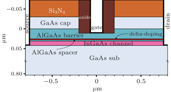
Figure 1 shows the typical device structure of the single-delta-doping GaAs PHEMT[15] utilized in this paper. Above the InGaAs channel layer is the delta-doping layer, which provides the carriers for the InGaAs channel layer. In order to reduce the coulomb impurity scattering, which influences the electronic mobility, an AlGaAs spacer layer is sandwiched between the delta-doping layer and the InGaAs channel layer. Here, the gate length is 0.25 μm and the Schottky barrier height is 0.9 eV. The thermal electrode is on the bottom side where the lattice temperature maintains 300 K, and the thermal boundary conditions at other boundaries are adiabatic.
Fig. 1. Typical structure of the single delta-doping GaAs PHEMT.
2.2. Numerical model
To simulate the burning process of the device under the EMP injection, it is needed to consider the electro–thermal effect. Here the Thermodynamic model and Hydrodynamic model are activated to simulate the carrier transport process. In addition to the Poisson equation and carrier continuity equations, the carrier temperature and heat flow equations are also solved. The Avalanche model accounting for impact ionization and AnalyticTEP model for thermal electric power are all taken into account in this work.
2.3. Signal model
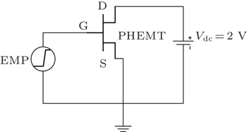
At present, in the study of the damage effect on the semiconductor device with the EMP event, researchers always take the step voltage pulse as the EMP signal model.[6,8,12] Figure 2 shows the simulation circuit in this study. The GaAs PHEMT device is injected by the step voltage pulse with a rising time of 1ns and an amplitude of 6 V on the gate. Here, the drain and the source are applied with 2 V and grounded, respectively. The device failure is indicated when the lattice temperature reaches the melting point of GaAs at 1511 K.
3.1. Distribution and variation of the electric field
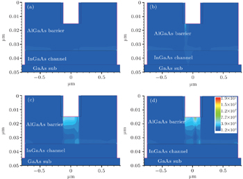
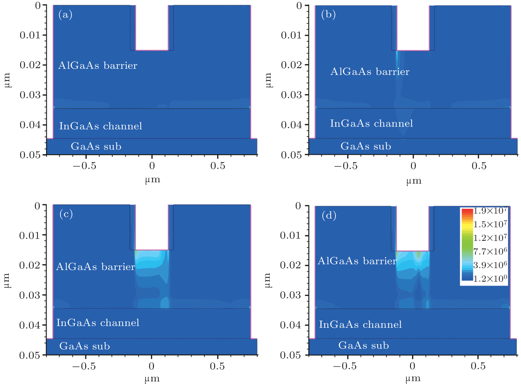
Figure 3 shows the distributions of the electric field at various times. When the gate electrode is injected with the step voltage pulse, the Schottky junction is forward-biased and the heterojunction reverse-biased. The electric field peaks are located at the interface of the heterojunction initially (Fig. 3(a)). With the increase of time, when the injection voltage reaches the threshold voltage of the Schottky junction, the gate current increases exponentially with the injection voltage increasing.[16] Owing to the low doped barrier layer, the gate–source and gate–drain voltages mostly drop on the barrier layer. Considering the potential differences between the gate electrode and the other two electrodes, the electric field peaks appear beneath the gate near two sides and the maximum electric field occurs near the source (Fig. 3(b)). When the voltage injected on the gate increases to a certain value, the electric field strength below the gate reaches the critical electric field, resulting in the avalanche breakdown, and causes the carriers to increase rapidly. With the time increasing, the electrons beneath the gate near two sides can be transferred quickly due to the high electric field, and below the gate center the electrons begin to accumulate. The electron accumulation effect causes the electron density beneath the gate center to be higher than those at other positions, which results in the shift of the electric field to the center of the barrier layer under the gate (Fig. 3(c)),[15] thereby forming an electric field peak under the gate center near the drain at the burnout (Fig. 3(d)).
Fig. 3. Distributions of the electric field (V/cm) at various times: (a) t = 0.4 ns, (b) t = 0.8 ns, (c) t = 1.4 ns, and (d) t = 2.34 ns.
3.2. Distribution and variation of the current density
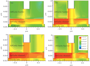
Figure 4 illustrates the distributions of the current density at various times. When the injection voltage is lower than the threshold voltage of the Schottky junction, the gate current is very small and most of the source electrons flow into the drain (Fig. 4(a)). As the voltage injected on the gate exceeds the threshold voltage of the Schottky junction, the gate current increases rapidly, which causes a current path to emerge between the gate and the InGaAs channel layer (Fig. 4(b)). Once the increased injection voltage makes the local electric field reach the critical electric field of avalanche breakdown, the gate current increases more quickly. With the increase of the time, the distribution of the current density begins to extend to the center of the barrier layer under the gate due to the shift of the electric field to this position(Fig. 4(c)), and finally results in a peak beneath the gate center near the drain (Fig. 4(d)).
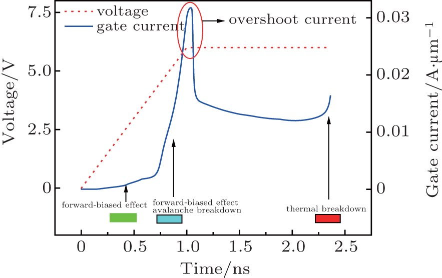
Figure 5 shows the response of the gate current in the damage process of the step voltage pulse. There are three mechanisms, i.e., forward-biased effect, avalanche breakdown, and the thermal breakdown, to influence the variation of the gate current. Meanwhile, it can be seen that there exists a current overshoot phenomenon at the end of the rise time.[17,18] In Ref. [17] it is explained that the overshoot current is due to the capacitive performance of the device under high frequency, which is a complex physical behavior. Here the authors do not conduct a more in-depth study on the mechanism of the current overshoot phenomenon.
Fig. 5. Response of the gate current with the time.
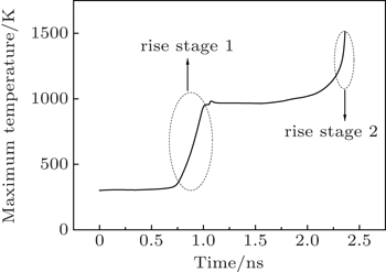
3.3. Distribution and variation of the temperature
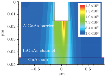
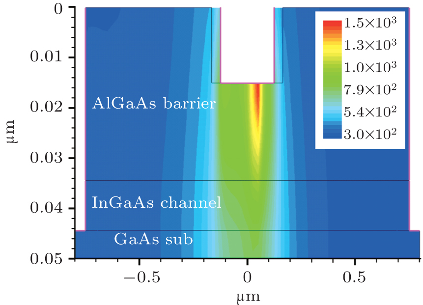
In the damage phenomenon of the semiconductor device induced by the external EMI, the temperature is an important assessment parameter, which is directly related to the device performance and reliability. Based on the power density Q = J ·E, the maximum temperature depends on current density J and electric field E. Figure 6 shows the response of the maximum temperature of the device during the injection of the step voltage pulse. It can be seen from this figure that there are two rise stages of the maximum temperature in the whole process. During the rise period of the injected pulse, the applied voltage and gate current increase with time increasing simultaneously (Fig. 5), which causes the maximum temperature to rise sharply. When the injection voltage reaches a steady value, the gate current varies little with time (Fig. 5), resulting in a constant stage of the maximum temperature. With the increase of time, the thermal breakdown happens when the device absorbs a certain energy, which causes the gate current and consequently the maximum temperature to rise sharply again. It should be noted that the final burnout of the device is due to thermal breakdown. Figure 7 illustrates the distribution of the temperature at the burnout time. It can be seen that the maximum temperature appears beneath the gate near the drain, which is easily understood since both the peaks of the electric field and the current density are at this position (Figs. 3(d) and 4(d)).
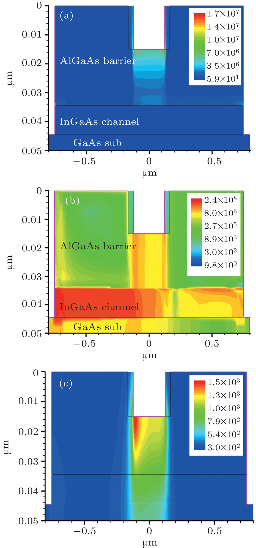
Fig. 8. Distributions of the device parameters under 10-V injection voltage: (a) electric field (V/cm), (b) current density (A/cm2), and (c) temperature (K).
Figure 8 shows the distributions of the electric field, the current density, and the temperature of the device under the injecting pulse with an amplitude of 10 V at the moment of burnout. It can be seen that the device has been damaged when the electric field began to extend to the center of the barrier layer but did not form the electric field peak. So the maximum temperature position is beneath the gate near the source at the burnout (Fig. 8(c)), which is different from that of the low amplitude of the injection pulse (Fig. 7).
3.4. Comparison with experimental results
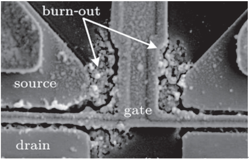
An experiment on the damage effect of the GaAs PHEMT subjected to the HPM was done in Ref. [14]. The device used in the experiment has the same structure of the delta-doping AlGaAs/InGaAs heterojunction as that in the simulation model in this paper, and a microwave signal is injected on the gate electrode with the drain biased 2 V and source grounded. Experimental results show that the device damage is beneath the gate near the source (Fig. 9), which coincides with the simulation results of the device under the high amplitude of the step voltage pulse in this paper (Fig. 8(c)). However, it cannot be avoided that the damage position of the device will also appear under the gate near the drain with the low amplitude of the step voltage pulse. Meanwhile, it can be seen that the gate current increases rapidly in the damage process of the EMP as indicated by the previous analysis of the current density, especially at the end of the rise time. This phenomenon may cause another damage to the gate metal strip melting, which has been found experimentally.[15] It should be pointed out that the gate position is the weak areas of the device regardless of the fact that the device damage is due to the semiconductor material burnout or the gate metal strip melting. So, in the external EMI assessment and hardening programs, the designer should pay more attention to the gate location. Although the pulse signal in this simulation is different from the microwave pluses applied in the experiment, it should be noted that the device damage caused by the microwave signal is due to the energy accumulation,[14] which is similar to the damage effect under the action of the step pulse voltage in this study. These failures induced by the two different signals both result from the thermal breakdown after the device has absorbed enough energy, which has a certain similarity to the device with the same structure and injection location. The comparison between simulation results and experimental ones shows that the device damage model presented in this paper can predict the damage effect of the EMP on the GaAs PHEMT well.
Fig. 9. Interior features of damaged device with microwave pulse.[14]
4. Conclusions
In this paper, the damage process of the EMP on the GaAs PHEMT is investigated. Simulation results show that the gate current increases rapidly under the injection of the step voltage pulse on the gate electrode, because of the forward-biased effect of the Schottky junction, the avalanche breakdown and the thermal breakdown of the barrier layer. It is observed that the damage position is different with the different amplitude of the step voltage pulse. When the amplitude of the pulse is low, the damage will appear under the gate near the drain; when the amplitude is high enough the damage will appear under the gate near the source, which is in agreement with the experimental result. At the same time, due to the higher gate current, especially the current overshoot phenomenon, the damage induced by the metal strip melting must also be paid more attention to. Which one of whether the semiconductor material burnout or the gate metal strip melting appears first, still needs further study. The results presented in this paper have a certain reference value to the EMP assessment and hardening programs of the LNA circuit.


 , Chai Chang-Chun1, Zhao Gang2, Yang Yin-Tang1, Yu Xin-Hai1, Liu Yang1]