1. IntroductionIn pursuit of a faster response speed and lower power consumption in field effect transistors, the channel length becomes smaller and smaller, and so does the thickness of gate dielectric.[1] Two-dimensional atomic-layered channel materials such as monolayer MoS2[2] have attracted a great deal of attention recently, and the FETs fabricated with them exhibit high carrier mobility and excellent on/off current ratio.[3] However, wide application is impossible without the same atomic-layered dielectrics, which have rarely been reported. Here, we investigate the single layer two-dimensional Ta2O5 that can function as a gate dielectric.[4] Compared with conventional SiO2, on which the carrier mobility is limited by scattering from surface optical phonons or charged surface states and impurities,[5] Ta2O5 has many superior properties including a high dielectric constant,[4] large refractive index value,[6] as well as high chemical and thermal stability,[7] etc.
Single layer Ta2O5 can be obtained via assembling Ta2O5 nanosheets, i.e., the so-called sequential adsorption method.[8–10] Nanosheets have an ultrathin thickness of 0.5 nm–3 nm and a lateral size of micrometers range, meaning that they are composed entirely of surface atoms and thus can be regarded as a unique class of two-dimensional nanoscale materials possessing properties such as single-crystalline quality, well-defined chemical composition, and extremely high anisotropy.[9–12] Pioneering work has been done on the oxide nanosheets and they show excellent electronic and magnetic properties including high dielectric constants and gigantic magneto–optical effects compared with conventional nanocrystallites and bulk materials.[10,13]
Ta2O5 nanosheets can be used as building blocks to fabricate nanostructured materials applied to electronic devices. However, the electronic performance could be seriously affected by various defects.[14–16] Some defects occur because of the diffusion of oxygen into tantalum, resulting in interstitial oxygen defects, and oxygen substoichiometry, resulting in oxygen vacancies.[17,18] Due to these defects, leakage current will occur in the oxide gate dielectric layer. Therefore, the investigation of defect properties in Ta2O5 nanosheets is of significant importance. Deep-level transient spectra (DLTS) and thermally stimulated current (TSC) are two general methods used to measure the electrical levels of thin-film defects. Since the former needs to form an Ohmic contact for the sample bottom electrode and the latter is mostly used for powder or liquid, they are unsuitable for nanosheets. Nondestructive and noncontact spectroscopic ellipsometry (SE) can detect the defect states and energy levels of high-κ film, which has been proposed in previous work.[18] Ellipsometry can investigate the dielectric properties of thin film by detecting the phase information and polarization state of light, and the thickness measurement can reach angstrom resolution.[19–21]
In this paper, the fabrication of single layer two-dimensional Ta2O5 via assemblies of nanosheets is introduced in the beginning, and then atomic force microscopy (AFM), x-ray photoelectron spectroscopy (XPS), and SE fitting are performed on samples. A key feature of this paper is the use of SE to investigate the electrical defects levels of single layer Ta2O5. The electrical levels of different charged oxygen vacancies will be shown by detailed SE fitting using the Lorentz oscillator model.
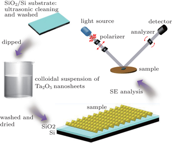
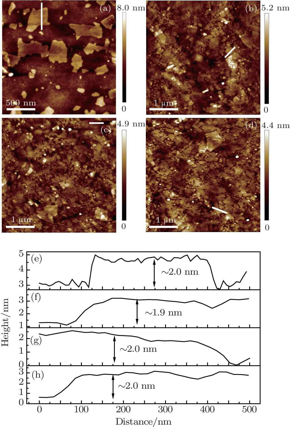
3. Results and discussionFigure 2 shows AFM images of different samples, including (a) dipped in a colloidal suspension of Ta2O5 nanosheets for 2 minutes and (b)–(d) dipped for 20 minutes for sample 1, 2, and 3, respectively. Samples 1–3 were prepared under the same experimental conditions for repeatability. The top column of Fig. 2 depicts the surface morphologies of samples while the bottom column shows the edge thicknesses of samples along the marked lines in panels (a)–(d). Nanosheets distribute dispersedly on the surface of substrates for samples dipped for 2 minutes, nevertheless for samples dipped for 20 minutes they have covered most of the surface and thus can be regarded as layered two-dimentional Ta2O5. These nanosheets have a thickness of ∼ 2 nm and a lateral size of several hundred nanometers. Compared with ∼ 1-nm thick unilamellar Ta2O5 nanosheets,[11,12] the difference between the experimental height and crystallographic thickness may stem from adsorbed charge-compensating protons, oxonium ions or water molecules, as is the case for other nanosheets.[8,12] Additionally, in order to exclude the influences of acetone and alcohol, samples were annealed at 300 ˚C, 400 ˚C, and 500 ˚C, respectively, then AFM was measured again to verify the edge thickness variation. There was no significant change, proving that the thickness difference is not from acetone and alcohol.
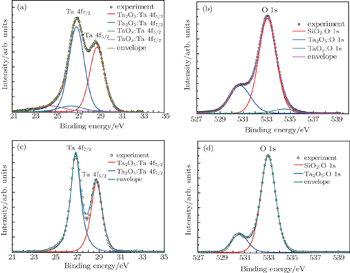
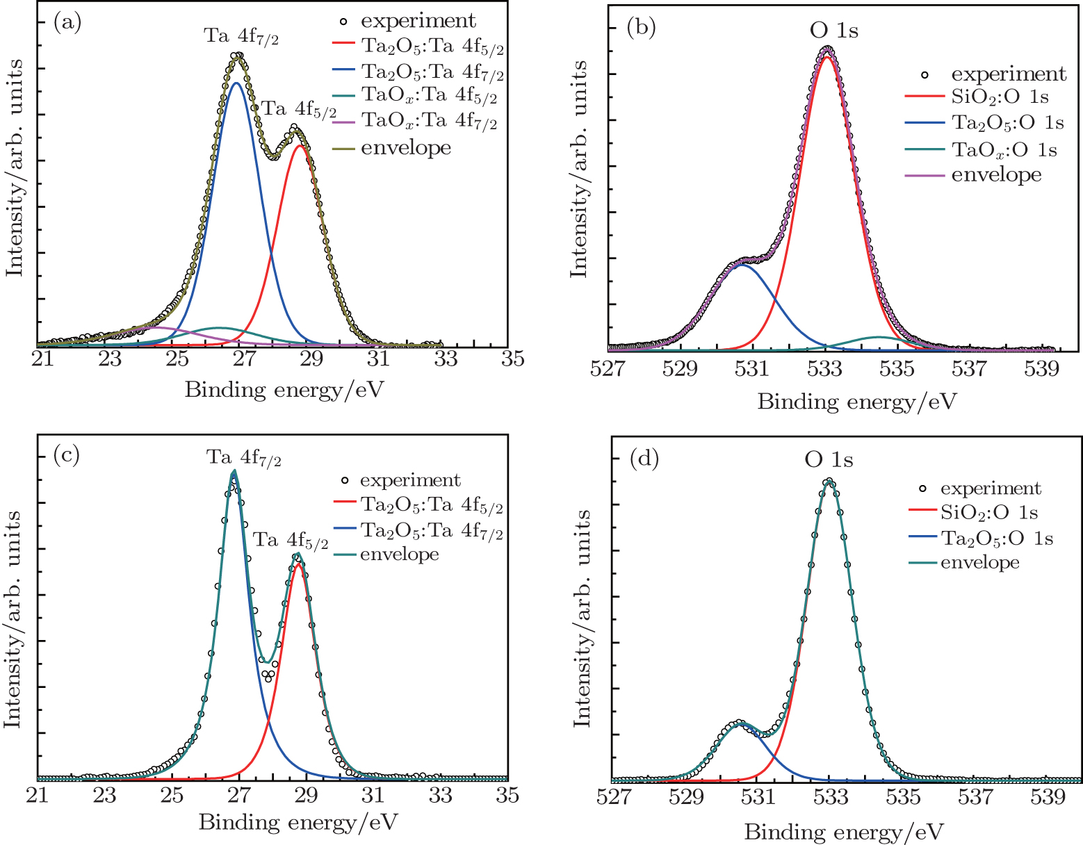
To characterize the chemical state of the single layer Ta2O5, XPS analysis was performed on samples dipped for 20 minutes. Figure 3 illustrates the Ta 4f and O 1s spectra. The black circles represent the as-recorded data. The Ta 4f signal (Fig. 3(a)) is fitted with four peaks. Peaks located at 26.88 eV and 28.77 eV (energy separation of 1.89 eV, area ratio of 1.36, and FWHM values of 1.66 eV and 1.61 eV, respectively) are representative for TaTa2O5 4f7/2 to TaTa2O5 4f5/2 spin orbital splitting, consistent with previous results.[22] Peaks located at 24.48 eV and 26.37 eV (energy separation of 1.89 eV) refer to TaTaOx 4f7/2 and TaTaOx 4f5/2 in the tantalum sub-oxide state, respectively.[23] Oxygen vacancies are closely related to the formation of tantalum sub-oxides that lead to oxygen non-stoichiometry.[17] The O 1s spectrum (Fig. 3(b)) can actually be fitted with three Gaussion components: OTa2O5 1s peak at 530.7 eV, OSiO2 1s peak at 533.05 eV and OTaOx 1s peak at 534.48 eV, supported by values in other articles.[24,25] The calculated [O]/[Ta] atomic ratio is 1.98 on the basis of the above analysis, smaller than the theoretical value of 2.5. Therefore, the defect levels of oxygen vacancies exist in as-grown single layer Ta2O5. As a control, rapid thermal process (RTP) was performed on samples dipped for 20 minutes in pure oxygen atmosphere at 700˚ for 5 minutes, and XPS was also measured, as shown in Fig. 3(c) and Fig. 3(d). Peaks of Ta 4f signal for the annealed sample are located at 26.84 eV and 28.76 eV (energy separation of 1.92 eV, area ratio of 1.4, and FWHW values of 1.09 eV and 1.21 eV, respectively), and peaks of O 1s signal are located at 530.58 eV and 533.02 eV, all of which match well with the corresponding peaks for the unannealed sample. In addition, the calculated [O]/[Ta] atomic ratio is 2.47. Therefore, the disappearance of the tantalum sub-oxide state proves the previous conclusion effectively, and oxygen vacancies can be strongly suppressed by annealing in a pure oxygen atmosphere.
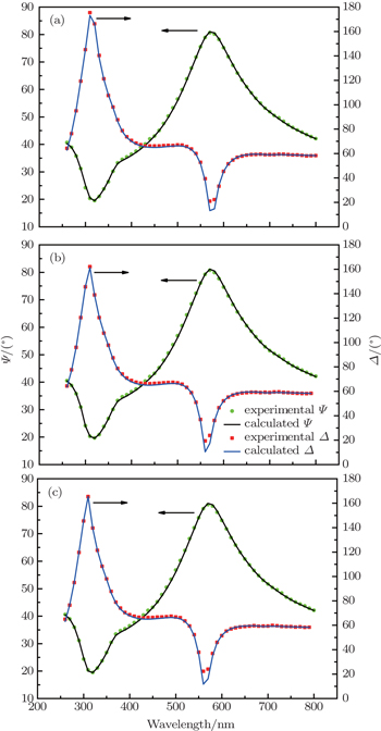
To investigate the defect states and energy levels of single layer Ta2O5, we measured SE of samples 1–3, as shown in Fig. 4. The ellipsometric parameters Ψ and Δ are related to optical and structural properties of the samples and are defined as:

where
rp and
rs represent the complex reflection coefficients of polarized light parallel and perpendicular to the incidence plane, respectively.
[18,26–28] The SE spectra were analyzed by a four-phase model of Si substrate/SiO
2 layer/Ta
2O
5 layer/ambient, and unknown parameters, i.e., film thickness (
d) and dielectric constant (
ε) for single layer Ta
2O
5, are defined as fitting variables.
The XPS results indicate that oxygen vacancies exist in as-grown single layer Ta2O5, thus the measured SE data can be fitted by adopting the Lorentz oscillator model to characterize the dispersion model of the Ta2O5 layer described as follows:

where
ε∞ is the light-frequency dielectric constant.
Ai,
Ci, and
νi are the amplitude representing the proportion of oscillator
i to the whole system, the center energy representing the transition energy, and the damping coefficient of each oscillator in unit eV, respectively.
Three oscillators are used in the data analysis with key parameters listed in Table 1. Curves calculated using the Lorentz oscillator model described above fit well with the experimental results, as shown in Fig. 4. In addition, the thickness of samples 1–3 measured from AFM is about 2 nm. Compared with the SE fitting results, these values exhibit good agreement, confirming that the Lorentz oscillator model is an appropriate analytical dispersion model for these samples.
Table 1.
Table 1.
 Table 1. Main parameters of the fitting results for all samples using the Lorentz oscillator model. .
|
Sample |
|
1 |
2 |
3 |
| d/nm |
1.92 |
1.95 |
1.98 |
| A1/eV |
3.13 |
2.65 |
2.84 |
| C1/eV |
5.14 |
5.19 |
5.17 |
| A2/eV |
0.88 |
0.63 |
0.08 |
| C2/eV |
4.00 |
4.06 |
4.09 |
| A3/eV |
9.24×10⁻⁴ |
7.30×10⁻⁶ |
1.90×10⁻⁵ |
| C3/eV |
2.14 |
2.18 |
2.18 |
| Table 1. Main parameters of the fitting results for all samples using the Lorentz oscillator model. . |
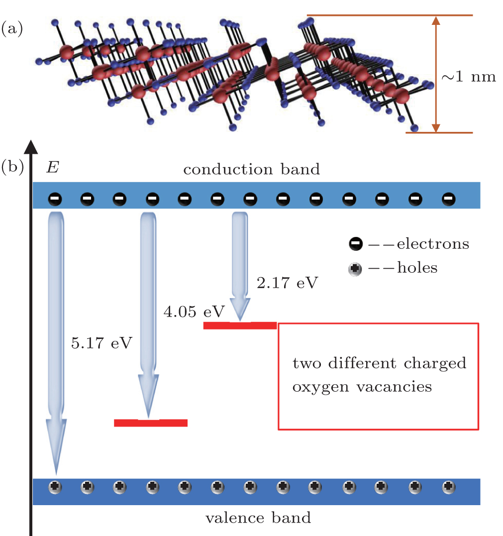
The oscillator energies Ci for all samples converge to three dominant values, with averages of 5.17, 4.05, and 2.17 eV, as listed in Table 1. Due to the size quantization effects, the optical bandgap energy of unilamellar Ta2O5 nanosheets can be derived as about ∼ 5.3 eV,[11,12] much larger than that of bulk Ta2O5, about ∼ 4 eV.[29] The oscillator center energy of 5.17 eV is very close to the bandgap transitions of Ta2O5 nanosheets, thus C1 can be regarded as the bandgap energy, and the discrepancy can be explained by the different thicknesses. Pioneering work indicates that the oxygen vacancies in Ta2O5 can cause a defect level in the energy gap at ∼ 2 eV, close to center energy C3, and different defect levels are assigned to electrons trapped at different charged oxygen vacancies from the bottom of the conduction band.[17,18] With regard to the center energy C2, considering that the as-grown Ta2O5 is too thin and SiO2 is transparent in the range of 260 nm–800 nm, the absorption of substrate Si cannot be ignored, and thus C2 is possible from that absorption. Although Si has a critical point absorption peak at ∼ 4.25 eV,[30] the ∼ 0.2 eV difference between the absorption peak and C2 is slightly larger, and the location of absorption peak is steady for Si, which demonstrates that the previous assumption is invalid, in other words, C2 does not result from Si. Combined with the XPS results, the center energies of 2.17 eV and 4.05 eV can be explained as two different charged oxygen vacancies.[17,18] Figure 5(a) shows a three-dimensional schematic representation of the Ta2O5 atomic structure consulted from other works,[11,12] and figure 5(b) shows the band structure of single layer two-dimensional Ta2O5 on the basis of the SE fitting results.
According to the definition of the Lorentz oscillator model, parameter Ai expresses the probability of the electronic transitions from the conduction band to the valence band or defect traps. From Table 1, the value of A1, corresponding to the bandgap oscillator, is larger than values of A2 and A3, indicating that the bandgap transition is most probable. Both A2 and A3 are very small values, but A2 is much larger than A3, which gives a conclusion that the defect energy of 4.05 eV is the dominant defect configuration, thus peaks corresponding to defect level C3 are invisible in XPS spectra. Additionally, A2 of sample 3 is approximately one order of magnitude smaller than that of samples 1 and 2, therefore, the probability of the electronic transitions from the conduction band to defect level C2 in sample 3 is also smaller than that in samples 1 and 2.


 , Chen Liangyao1, Zhang David Wei2, Zhou Peng2, ‡,