Study on electrical defects level in single layer two-dimensional Ta2O5
Li Dahai1, Song Xiongfei2, Hu Linfeng3, Wang Ziyi1, Zhang Rongjun1, †,  , Chen Liangyao1, Zhang David Wei2, Zhou Peng2, ‡,
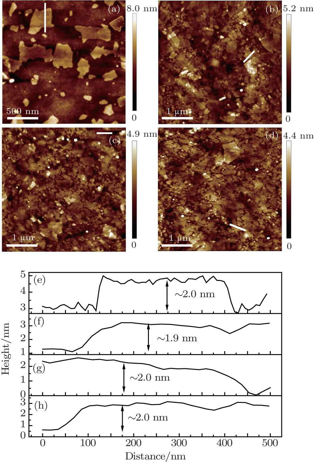
, Chen Liangyao1, Zhang David Wei2, Zhou Peng2, ‡, AFM images of Ta2O5 nanosheets deposited on SiO2/Si substrates. The top is the surface morphologies of different samples: (a) dipped in a colloidal suspension of Ta2O5 nanosheets for 2 minutes and dipped for 20 minutes for (b) sample 1, (c) sample 2, and (d) sample 3. The bottom is the height profile of marked lines in panels (a), (b), (c), and (d), respectively.