


Effect of gate length on breakdown voltage in AlGaN/GaN high-electron-mobility transistor
[Luo Jun1, Zhao Sheng-Lei1, Mi Min-Han1, Chen Wei-Wei2, Hou Bin2, Zhang Jin-Cheng1, Ma Xiao-Hua1, 2, Hao Yue1, †,  ]
]
]
|
|


† Corresponding author. E-mail:
Project supported by the National Natural Science Foundation of China (Grant Nos. 61334002, 61106106, and 61204085).
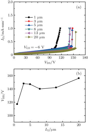
The effects of gate length LG on breakdown voltage VBR are investigated in AlGaN/GaN high-electron-mobility transistors (HEMTs) with LG = 1 μm∼ 20 μm. With the increase of LG, VBR is first increased, and then saturated at LG = 3 μm. For the HEMT with LG = 1 μm, breakdown voltage VBR is 117 V, and it can be enhanced to 148 V for the HEMT with LG = 3 μm. The gate length of 3 μm can alleviate the buffer-leakage-induced impact ionization compared with the gate length of 1 μm, and the suppression of the impact ionization is the reason for improving the breakdown voltage. A similar suppression of the impact ionization exists in the HEMTs with LG > 3 μm. As a result, there is no obvious difference in breakdown voltage among the HEMTs with LG = 3 μm∼20 μm, and their breakdown voltages are in a range of 140 V–156 V.
Owing to their high two-dimensional electron gas (2DEG) density, electron mobility, and high breakdown electric field, AlGaN/GaN high-electron-mobility transistors (HEMTs) have become excellent candidates in power electronics and high frequency applications.[1–6] The value of gate length has influences on transconductance, cutoff frequency, and maximum frequency of oscillation.[7,8] Numerous studies focused on reducing the gate length to improve high-frequency characteristics.[9,10] Breakdown voltage is also a very important parameter for these applications. However, the effect of gate length LG on breakdown voltage VBR has rarely been investigated.
In this paper, the effect of gate length on breakdown voltage is investigated through experiments and simulations. With the increase of LG, VBR is first increased, and then saturated at LG = 3 μm. In order to explain the relation between VBR and LG, leakage currents and software simulation are utilized to discuss the buffer leakage current and buffer-leakage-induced impact ionization.
Figure
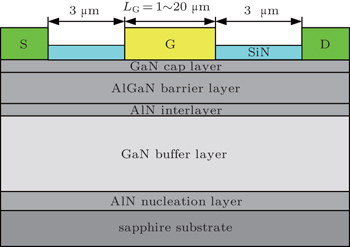
 | Fig. 1. Schematic cross section of AlGaN/GaN HEMT. |
Source and drain electrodes were formed by evaporating Ti/Al/Ni/Au followed by annealing in N2 ambient at 830 °C for 30 s. Then, mesa isolation was carried out by Cl-based reactive ion etching (RIE). Next, a Schottky gate was formed by evaporating Ni/Au/Ni. The devices were passivated with SiN layers to reduce surface states. The gate-source spacing and gate-drain spacing are all 3 μm. Six kinds of devices were fabricated with different gate length LG values, and the gate length values are 1, 3, 5, 8, 13, and 20 μm.
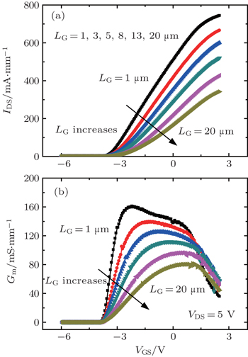
The source–drain spacing increases with the increase of gate length from 1 μm to 20 μm, leading to the increase of on-state resistance. As a result, the maximum drain current IDmax decreases with the increase of gate length. As shown in Fig.
 | Fig. 2. I–V transfer characteristics of the AlGaN/GaN HEMTs with different gate length values: (a) IDS versus VGS and (b) Gm versus VGS. |
Figure
 | Fig. 3. (a) Breakdown characteristics and (b) VBR–LG dependence of the AlGaN/GaN HEMTs with different gate length values. |
Figure
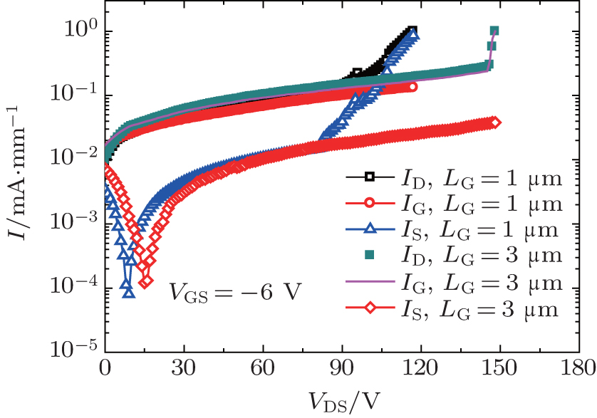 | Fig. 4. Variations of ID, IG, and IS with VDS (drain–source voltage) during the breakdown measurements in HEMTs with LG = 1 μm and LG = 3 μm. |
 | Fig. 5. Off-state leakage currents in AlGaN/GaN HEMTs during the breakdown measurements. Gate leakage current IG consists of source–gate leakage current Isg and drain–gate leakage current Idg. |
As shown in Fig.
Figures
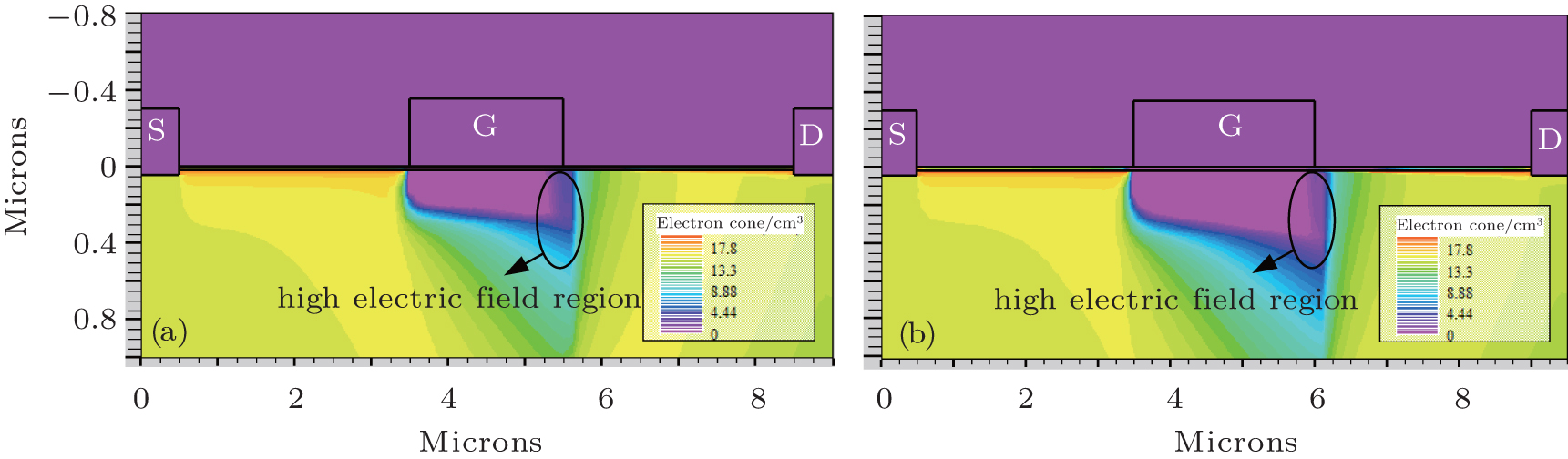
 | Fig. 6. Off-state logarithmic electron concentration distributions of the AlGaN/GaN HEMTs respectively with (a) LG = 1 μm, VDS = 0 V; (b) LG = 1 μm, VDS = 100 V; (d) LG = 3 μm, VDS = 0 V; (e) LG = 3 μm, VDS = 100 V. Electric field distributions of the AlGaN/GaN HEMTs respectively with (c) LG = 1 μm, VDS = 100 V; (f) LG = 3 μm, VDS = 100 V. All the devices are biased at VGS = −6 V and simulated by Silvaco-ATLAS software. |
With the drain biased at a high value, there exists an electric field peak at the drain-side edge of the gate terminal as shown in Figs.
The breakdown for the HEMT with LG = 1 μm belongs to buffer-induced breakdown. The suppression of the buffer leakage changes the breakdown type into gate-induced breakdown for the HEMT with LG = 3 μm. For the gate length larger than 3 μm, the high electric field region is almost completely depleted, which is similar to the case of LG = 3 μm. A similar suppression of the impact ionization exists in each of the HEMTs with LG > 3 μm. For the HEMTs with LG = 5, 8, 13, and 20 μm, the device breakdown types are all gate-induced breakdown. As shown in Table
| Table 1. Parameter values of AlGaN/GaN HEMTs. The threshold voltage Vth is defined as the gate voltage with drain leakage current reaching 1 mA/mm. The gate leakage current Igleak values are obtained at VGS = −15 V. . |
In order to find out the accurate gate length in which the buffer-leakage-induced impact ionization can be alleviated, the simulation for the HEMT with LG = 2 μm is carried out, and the results are shown in Fig.
 | Fig. 7. Off-state logarithmic electron concentration distributions of the AlGaN/GaN HEMTs respectively with (a) LG = 2 μm, VDS = 100 V; (b) LG = 2.5 μm, VDS = 100 V. |
In this work, the effects of gate length on breakdown voltage are investigated in AlGaN/GaN HEMTs. The value of VBR for the HEMT with LG = 3 μm is 148 V, which is 31 V higher than that for the HEMT with LG = 1 μm. For the HEMT with LG = 3 μm, the high electric field region is almost completely depleted, and it is difficult to inject the electrons from the source into the high electric field region. The gate length of 3 μm can alleviate the buffer-leakage-induced impact ionization compared with the gate length of 1 μm, and the suppression of the impact ionization is the reason for improving the breakdown voltage. A similar suppression of the impact ionization exists in each of the HEMTs with LG > 3 μm, and there is no obvious difference in breakdown voltage among the HEMTs with LG = 3 μm–20 μm. Simulation results indicate that the gate length value in which buffer-leakage-induced impact ionization begins to be alleviated is in a range between 2 μm and 2.5 μm.
| 1 | |
| 2 | |
| 3 | |
| 4 | |
| 5 | |
| 6 | |
| 7 | |
| 8 | |
| 9 | |
| 10 | |
| 11 |