†Corresponding author. E-mail: x.guo@sjtu.edu.cn
‡Corresponding author. E-mail: shunwang@sjtu.edu.cn
§Corresponding author. E-mail: yingl@sjtu.edu.cn
*Project supported by the Natural Science Foundation of Shanghai, China (Grant No. 13ZR1456800), Ph. D. Programs Foundation of Ministry of Education of China (Grant No. 20120073110093), the National Natural Science Foundation of China (Grant Nos. 11274229, 11474198, 61274083, 61334008, 11274229, 11474198, 11204175), and DOE under DE-FG02-04ER46159.
Indacenodithiophene-co-benzothiadiazole (IDTBT) has emerged as one of the most exciting semiconducting polymers in recent years because of its high electronic mobility and charge transport along the polymer backbone. By using the recently developed ion gel gating technique we studied the charge transport of IDTBT at carrier densities up to 1021 cm−3. While the conductivity in IDTBT was found to be enhanced by nearly six orders of magnitude by ionic gating, the charge transport in IDTBT was found to remain 3D Mott variable range hopping even down to the lowest temperature of our measurements, 12 K. The maximum mobility was found to be around 0.2 cm2·V−1·s−1, lower than that of Cytop gated field effect transistors reported previously. We attribute the lower mobility to the additional disorder induced by the ionic gating.
Semiconducting polymers have generated great interest in recent years due to their potential applications in flexible electronics that can be processed from solution. An important goal for semiconductor polymer research is to improve the mobility of these polymers. The mobility in semiconducting polymers tends to be low because of the structural disorder. In the past decade, a lot of efforts have been devoted to design of polymers of high crytallinity. In crystalline and semicrystalline polymers such as reioregular poly-3-hexylthiophene (P3HT)[1] and poly(2, 5-bis(3-alkylthiophen-2-yl)thieno[3, 2-b]thiophene) (PBTTT), [2] high mobility is achieved because lamellar structure of π – π stacking backbone along the substrate normal (edge on) provides efficient charge transport pathways. Very recently, it has been found that several donor– acceptor co-polymers exhibit surprisingly high mobilities, [3] despite that they are much less structurally ordered than P3HT and PBTTT. Among them, indacenodithiophene-cobenzothiadiazole[4] (IDTBT) shows one of the highest mobilities, exceeding 1 cm2· V− 1· s− 1. Recent spectroscopic measurements and molecular dynamics calculations suggest a near-torsion-free IDTBT backbone, [5, 6] leading to low energetic disorder in IDTBT films. It is suggested that the charge transport in IDTBT is dominated by conduction along the "disorder-free" rigid backbone, where the disorder-induced carrier localization is very weak.
The mobility of the semiconducting polymer can be further enhanced by chemical doping. At low carrier concentration, the charge transport in semiconducting polymers is mainly thermally assisted hopping between localized electronic states, with very low mobility. Increasing carrier concentration by chemical doping leads to carrier delocalization and diffusive transport. In some bulk semiconducting polymers, for example, polyaniline[7, 8] and polypyrrole, [9] even metallic state has been achieved. More recently, ultra high carrier densities have been induced controllably over a wide range by electrochemical doping using ionic liquid/gel.[10, 11] This reversible process resembles the chemical doping. In ion gel gated P3HT transistors, the mobility reaches ∼ 1 cm2· V− 1· s− 1, compared to 0.1 cm2· V− 1· s− 1 in SiO2 gated field-effect transistors (FET). Moreover, Hall effect was observed in P3HT, indicating diffusive transport at high carrier densities.[12] In ionic liquid gated PBTTT transistors, mobility approaching 3 cm2· V− 1· s− 1 was also reported.[13]
In this paper we apply the ion gel gating technique to induce ultra-high carrier density in IDTBT.We successfully fabricated ion gel gated IDTBT thin film transistors, with on/off ratio approaching 106 in vacuum. The carrier mobility at carrier densities up to 1021 cm− 3 was found to be on the order of 0.1 cm2· V− 1· s− 1. To further understand the charge transport mechanism in IDTBT, we measured and analyzed the temperature dependence of resistivity at different carrier concentrations.
To fabricate the device, Cr (3 nm)/Au (25 nm) bottom electrodes were first patterned on SiO2/Si substrates using photolithography. IDTBT film was then spin-coated from a chlorobenzene solutions (5 mg· ml− 1) to a thickness of 27 nm, measured by an profilometer. The film was then manually patterned with a cotton swap under a microscope. Ion gel was spin coated on a glass substrate, cut with a razor blade and then laminated onto the SiO2/Si substrate. The ion gel solution was prepared by dissolving P(VDF– HFP) (purchased from Sigma– Aldrich) and [EMI][TFSI] (purchase from Sigma– Aldrich) in acetone. The weight ratio was P(VDF– HFP):[EMI][TFSI]:Acetone = 1:4:7. The details of the preparation of the ion gel can be found in Ref. [14]. Then the device was baked for 24 h at 70° C in N2 glove box.
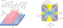
Figure 1(a) shows the chemical structure and schematic illustration of the “ face-on” orientations of the IDTBT backbone. To check the quality of our IDTBT film, we have fabricated the Cytop gated bottom contact IDTBT FET devices using the same method reported by Zhang et al.[5] The characteristics of transfer curves of the FET devices are similar to those reported in the literature and the room temperature mobility of the Cytop gated devices are ∼ 1.5 cm2· V− 1· s− 1, consistent with the previous reported values.[6] Figure 1(b) shows the schematic illustration of the ion gel gated IDTBT transistors. The electrodes were patterned into a Hall-bar geometry to carry out 4 terminal resistance and Hall effect measurements. In our devices, the contact area between the gate electrode and ion gel is comparable to or smaller than the area of the polymer, which leads to a difference between the voltage drop at the liquid/polymer and the applied voltage. The reason we have small size of the ion gel is that it is good for the mechanical stability of the device at low temperatures. We have carried out extensive experiments to prove that the small contact area between the gate electrode and ion gel is a not limiting factor for introducing ultra-high carrier density.
The two terminal ID− VG transfer curves of a typical ion gel gated IDTBT transistor measured in ambient condition area are plotted in Fig. 2(a). The device shows the characteristics of a p-type ion gel gated thin film transistor, with a large hysteresis, probably due to the slow motion of the ions and the side gating geometry. The small contact area of the gate electrode and the ion gel is also responsible for the hysteresis. It has been shown that reducing the thickness of the ion gel and employing top gate geometry could decrease the hysteresis.[15] The device is turned on at VG = 1.5 V, with an on/off ratio of nearly 104. The current at VG = − 2.0 V is ∼ 10 μ A. Sweeping VG beyond VG = − 2 V may cause degradation of the device. The color of the IDTBT film changes reversibly from blue at off state to transparent at on state, indicating that the bulk of the film is electrochemically doped. In vacuum, the turn-on voltage shifted to − 2.4 V, with an higher on/off ratio approaching 106 due to significant decrease in the off current. The shift in the turn-on voltage and a lower off current may both be explained by the removal of oxygen gas, which was known to serve as a p-type dopant in organic devices. The maximum ID is about the same as that in ambient.
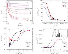
In order to determine the density and mobility of the carriers, the total injected charge Q was measured by integrating the gate current over a long time at room temperature. As an example, figure 3(a) shows the Q versus time with gate voltage VG changing from − 2.0 V to − 3.0 V for one device (Device 1). The carrier density was then estimated by p = Q/V, where V is the total volume of the IDTBT film, as shown in Fig. 3(b). If the film is uniformly doped, the charge carrier density can be estimated using the film thickness of 27 nm. The maximum carrier density achieved is 9 × 1020 cm− 3. The four-terminal conductivity σ as a function of VG is shown in Fig. 3(c). The maximum conductivity is about 8 S/cm at room temperature, lower than other ionic liquid/gel gated polymer transistors. The contact resistance in our devices was found to be 60 Ω · cm. The mobility changes from ∼ 6.0 × 10− 6 cm2· V− 1· s− 1 at VG = − 2.2 V to ∼ 0.1 cm2· V− 1· s− 1 at VG = − 3 V, as shown in Fig. 3(d). The data from two other devices (Devices 2 and 3) are also shown in Figs. 3(b)– 3(d), exhibiting similar carrier density, conductivity and mobility. The inset of Fig. 3(d) summarizes the maximum mobility of 32 devices. The maximum mobility in the ion gel gated IDTBT transistors are significantly lower than the mobility ∼ 1.5 cm2· V− 1· s− 1 in the Cytop gated devices.
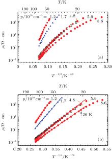
To gain more insight into the charge transport mechanism of ion gel gated IDTBT, we measured the temperature dependence of conductivity at different gate voltages down to 12 K for the three devices. Two types of variable-range hopping (VRH) conduction, Mott and Efros– Shklovskii VRH conductions are often observed in heavily doped polymers. In Mott VRH conduction, resistivity ρ = ρ 0 exp(T0/T)d + 1, where d is the dimensionality of the system.[16] The Efros– Shklovskii VRH is characterized by the exp(T0/T)2 behavior of the resistivity in all dimensions due to a soft-gapped density of states caused by Coulomb interaction.[17] Our data are plotted as ρ versus T1/2 and T1/4 in Fig. 4. The blue and red curves are from device 1 and 2 respectively. Our results clearly demonstrate 3D Mott VRH conduction at all measured gate voltages. As shown in Fig. 4, log (ρ ) is linear in T1/4 but not in T1/2, ruling out the Efros– Shklovskii and 1D Mott VRH. 1D transport was suggested by many groups working on Cytop gated IDTBT transistors based on the picture that the charge transport in this polymer is dominated by hopping along the backbone.[5, 6] The Hall effect measurements was also attempted at high carrier densities. However, no Hall effect was observed, which is consistent with the fact that the mobility of electrochemical doped IDTBT is low.
The lower mobility observed in ion gel gated IDTBT compared to Cytop gated FET is rather surprising. For P3HT and PBTTT, the carrier mobility are significantly higher in the ionic liquid/gel gated transistors than that in the conventional FET, where the carrier is usually an order of magnitude lower.[12, 13] In Cytop gated IDTBT, the high mobility relies on the low degree of backbone disorder due to resilience of the backbone conformation to side chain disorder.[6] The observation of 3D Mott VRH conduction at high carrier densities in our devices suggests that the charge transport mechanism is different from the Cytop gated FET. This is probably due to higher disorder induced by the penetration of ions. During the electrochemical doping process, the penetration of ions brings extra disorder into the polymer, which destroys the low disorder along the backbone, hindering the hopping along the backbone. Thus the carriers have to choose a less efficient pathway, i.e., the 3D hopping VRH transport, resulting in a lower mobility. It is also worthwhile to mention that, in organic single crystal such as rubrene and pentance where the disorder is low, it has been observed that gate dielectrics with higher polarizability reduces the mobility. The reason for such mobility decrease in single crystals is attributed to coupling of the charges in the channel with the polarizable dielectric.[18] The lower mobility we observed in IDTBT gated by ion gel compared to gated by Cytop could also be related to the fact that the disorder in IDTBT is indeed very low, which is consistent with the previous experiments and theories about IDTBT.
To summarize, we were able to tune the conductivity in IDTBT films by nearly six order of magnitude by ion gel gating. The maximum mobility of 0.2 cm2· V− 1· s− 1 is lower than that of the Cytop gated transistors. At high carrier densities, the charge transport mechanism is identified as 3D Mott VRH conduction. The suppression of mobility at high carrier density may be related to the doping induced disorder.
| 1 |
|
| 2 |
|
| 3 |
|
| 4 |
|
| 5 |
|
| 6 |
|
| 7 |
|
| 8 |
|
| 9 |
|
| 10 |
|
| 11 |
|
| 12 |
|
| 13 |
|
| 14 |
|
| 15 |
|
| 16 |
|
| 17 |
|
| 18 |
|


