Electronic mobility in the high-carrier-density limit of ion gel gated IDTBT thin film transistors

Electronic mobility in the high-carrier-density limit of ion gel gated IDTBT thin film transistors |
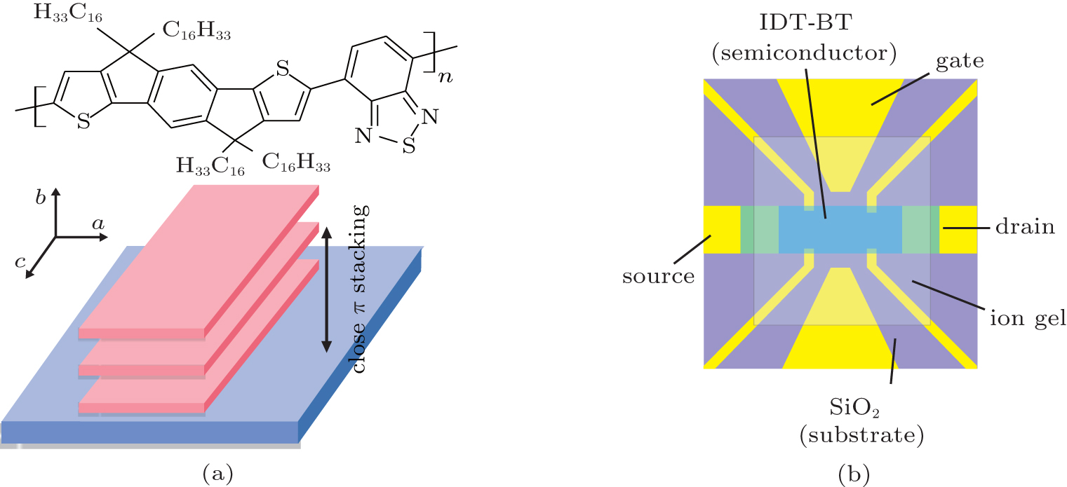
| (a) Molecular structure of IDTBT (top), and schematic illustration of the “face-on” orientations with red rectangular shapes denoting the conjugated backbone of the IDTBT thin film on the substrate. (b) top view of the ion gel gated device structure (with channel size of 500 μm × 1300 μm). |
 |