Yang Yi-Bin, Liu Ming-Gang, Chen Wei-Jie, Han Xiao-Biao, Chen Jie, Lin Xiu-Qi, Lin Jia-Li, Luo Hui, Liao Qiang, Zang Wen-Jie, Chen Yin-Song, Qiu Yun-Ling, Wu Zhi-Sheng, Liu Yang†, Zhang Bai-Jun‡. In-situ wafer bowing measurements of GaN grown on Si (111) substrate by reflectivity mapping in metal organic chemical vapor deposition system . Chinese Physics B, 24(9): 096103
Permissions
In-situ wafer bowing measurements of GaN grown on Si (111) substrate by reflectivity mapping in metal organic chemical vapor deposition system
Yang Yi-Bina),b), Liu Ming-Ganga),b), Chen Wei-Jiea),b), Han Xiao-Biaoa),b), Chen Jiea),b), Lin Xiu-Qia),b), Lin Jia-Lia),b), Luo Huia),b), Liao Qianga),b), Zang Wen-Jiea),b), Chen Yin-Songa),b), Qiu Yun-Linga),b), Wu Zhi-Shenga),b), Liu Yang†a),b), Zhang Bai-Jun‡a),b)
State Key Laboratory of Optoelectronic Materials and Technologies, Sun Yat-Sen University, Guangzhou 510275, China
School of Physics and Engineering, Institute of Power Electronics and Control Technology, Sun Yat-Sen University, Guangzhou 510275, China
*Project supported by the National Natural Science Foundation of China (Grant Nos. 61274039 and 51177175), the National Basic Research Program of China (Grant No. 2011CB301903), the Ph.D. Programs Foundation of Ministry of Education of China (Grant No. 20110171110021), the International Science and Technology Collaboration Program of China (Grant No. 2012DFG52260), the International Science and Technology Collaboration Program of Guangdong Province, China (Grant No. 2013B051000041), the Science and Technology Plan of Guangdong Province, China (Grant No. 2013B010401013), the National High Technology Research and Development Program of China (Grant No. 2014AA032606), and the Opened Fund of the State Key Laboratory on Integrated Optoelectronics, China (Grant No. IOSKL2014KF17).
Abstract
In this work, the wafer bowing during growth can be in-situ measured by a reflectivity mapping method in the 3×2″ Thomas Swan close coupled showerhead metal organic chemical vapor deposition (MOCVD) system. The reflectivity mapping method is usually used to measure the film thickness and growth rate. The wafer bowing caused by stresses (tensile and compressive) during the epitaxial growth leads to a temperature variation at different positions on the wafer, and the lower growth temperature leads to a faster growth rate and vice versa. Therefore, the wafer bowing can be measured by analyzing the discrepancy of growth rates at different positions on the wafer. Furthermore, the wafer bowings were confirmed by the ex-situ wafer bowing measurement. High-resistivity and low-resistivity Si substrates were used for epitaxial growth. In comparison with low-resistivity Si substrate, GaN grown on high-resistivity substrate shows a larger wafer bowing caused by the highly compressive stress introduced by compositionally graded AlGaN buffer layer. This transition of wafer bowing can be clearly in-situ measured by using the reflectivity mapping method.
PACS:
61.72.uj; 83.60.Hc; 61.72.Ff
Keyword:
stresses; metal organic chemical vapor deposition; wafer bowing; in-situ reflectivity mapping
The growth of GaN on silicon substrates has been extensively studied for the applications in optoelectronic devices and high-power electronic devices because of good properties of silicon, such as low cost, high quality, low hardness, good thermal conductivity, good electrical conduction, and large scale. Moreover, there is a potential of integrating conventional Si-based structures with group III-nitride films on a single wafer. However, the large thermal expansion coefficient (TEC) mismatch (56%) between GaN and Si (111) substrate results in great tensile stress and cracks in epilayers when the thickness is larger than 1.0 μ m. Thus, in the case of GaN-based compounds grown on Si, the stress is known to severely affect the device quality because of wafer bending, dislocation formation, or even cracks.[1] In order to counterbalance the tensile stress, many solutions have been researched such as low-temperature AlN (LT-AlN) interlayer, [2– 4] GaN/AlN superlattices structure, [5– 7] single AlGaN interlayer, [8, 9] step-graded AlGaN buffer layer, [10– 14] composition-graded AlGaN buffer layer, [15– 19] etc.
For all these techniques, it has been noticed that the growth parameters of the buffer layer or interlayer affect the quality of GaN greatly, which indicates that the precise optimization of the growth parameters and the detailed study of the stress relaxation mechanisms are essential.[17] Therefore, in-situ techniques play important roles during the growth process, which observes the stress evolution affected by the growth parameters. Among these in-situ techniques, most attention has been drawn to the LayTec’ sEpiCurve sensor, which measures the wafer curvature caused by stresses during the deposition of thin solid films. This technique is based on the measurement of the substrate curvature (usually in the center of the wafer) induced by the mismatch, because any mismatch strain (lattice, thermal, growth-induced mismatch, etc.) between film and substrate bends the whole system. Thus, this in-situ curvature measurement has already been widely applied to follow the stress evolution during metal organic chemical vapor deposition (MOCVD).[20– 27]
However, the LayTec’ sEpiCurve Sensor is too expensive. Thus, due to the lack of this measurement, we use a reflectivity mapping method to in-situ measure the wafer bowing during growth, which is usually applied to monitor the film thickness and growth rate. The wafer bowing caused by stresses (tensile and compressive) during the epitaxial growth leads to a temperature variation at different positions on the wafer, and the lower growth temperature leads to a faster growth rate and vice versa.[28– 30] Therefore, the wafer bowing can be measured by analyzing the discrepancy of growth rates at different positions on the wafer. In this paper, 0.9-μ m and 3-μ m GaN were grown on Si (111) substrates using an AlN seeding layer and the compositionally graded AlGaN buffer layer. The wafer bowing was in-situ measured by reflectivity mapping in the MOCVD system. The wafers showed concave bowing and convex bowing for 0.9-μ m and 3-μ m GaN grown on Si, respectively. These results were demonstrated by the ex-situ wafer bowing measurement. In comparison with high-resistivity Si substrate, GaN grown on low-resistivity substrate shows a smaller wafer bowing. It also can be in-situ measured by using this reflectivity mapping method. The similar result was reported by Dadgar et al., [31] in which the in-situ curvature measurement was used.
2. Experiment
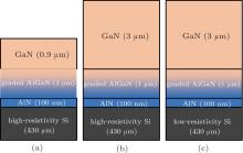
The growth of epilayers was performed in the 3 × 2″ Thomas Swan close coupled shower head MOCVD system. Trimethylgallium (TMGa), trimethylaluminum (TMAl), and ammonia (NH3) were employed as the reactant source materials for Ga, Al, and N, respectively. As substrates for epitaxial growth we used 430-μ m-thick high-resistivity (R > 1000 Ω · cm) Si (111) substrates for samples A and B, and 430-μ m-thick low-resistivity ( R < 0.02 Ω · cm, Sb-doped n-type) Si (111) substrate for sample C. As the epitaxial structures for these samples, shown in Fig. 1, an AlN seeding layer and a compositionally graded AlGaN buffer layer were deposited, followed by 0.9-μ m GaN for sample A and 3-μ m GaN for samples B and C. These three samples were all crack-free.
Fig. 1. Structures for (a) sample A, (b) sample B, and (c) sample C.
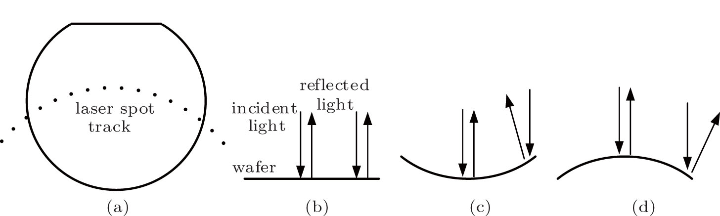
In the 3 × 2″ Thomas Swan close coupled shower head MOCVD system, the reflectivity measuring module combined with laser and detector is fastened to the shower head, with the wavelength of 635 nm. As shown in Fig. 2(a), with the rotation of the susceptor, the reflectivity of different points along a curve line can be detected, from the edge of the wafer to the center and to the edge again, rather than in the center only. Figure 2(b) shows that the reflected light is reflected back parallel to the incident light, no matter whether around the center or near the edge, when the wafer is flat. However, when the wafer bow is too concave or convex, the reflected light will be scattered to other directions, especially near the edge, which decreases the reflectivity intensity, as shown in Figs. 2(c) and 2(d).
Fig. 2. (a) The schematic diagram of the track of laser spot, which is a curve, with the rotation of the susceptor. (b)– (d) Directions of incident light and reflected light related with the wafer bow.
3. Results and discussion
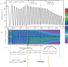
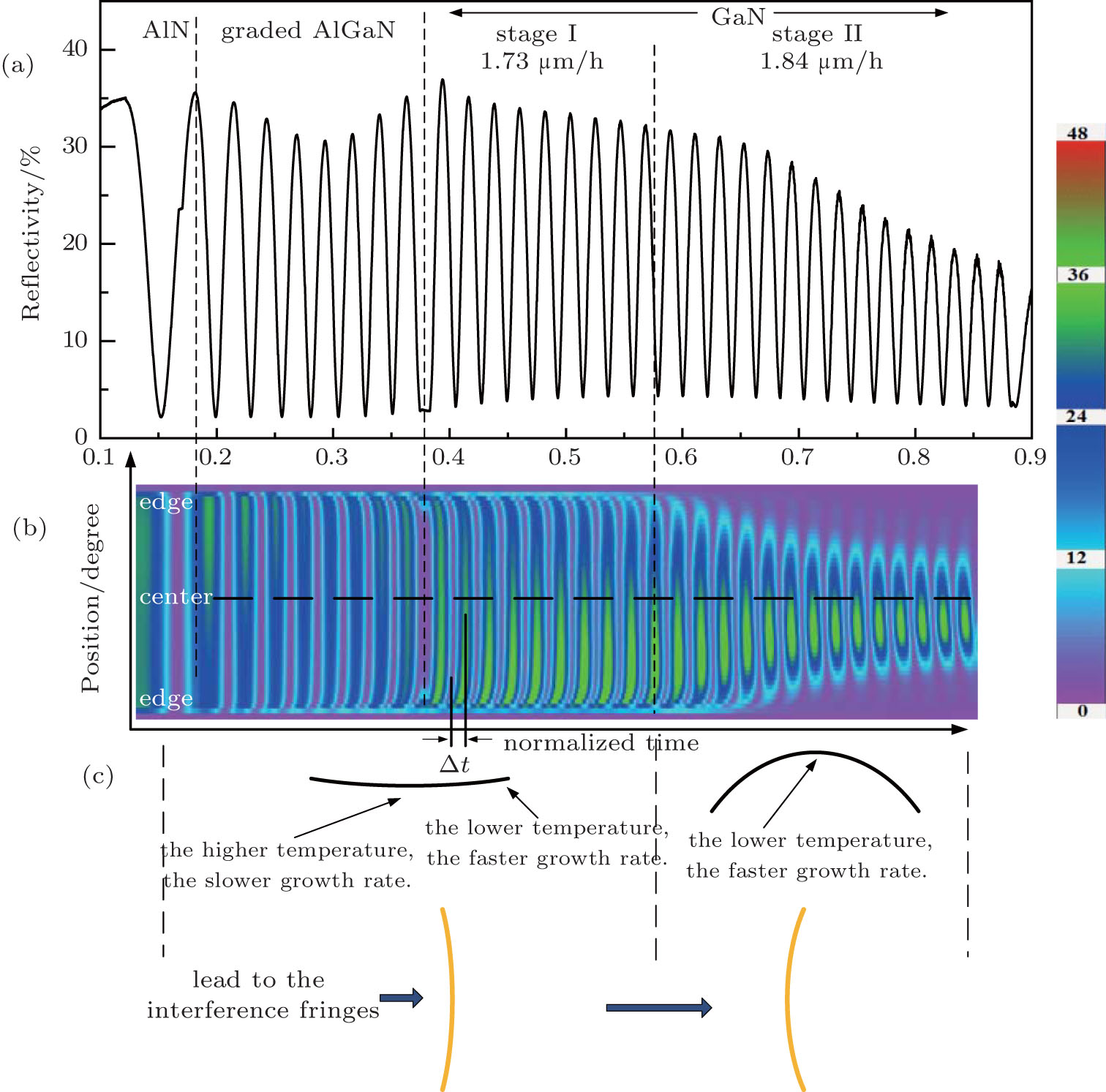
In Fig. 3, the relation of reflectivity (Fig. 3(a)), reflectivity mapping (Fig. 3(b)), and schematic diagrams (Fig. 3(c)) of wafer bows and interference fringes changing are clearly shown. With the rotation of the susceptor, the reflectivity of different positions under the track of the laser spot is detected, forming each interference fringe in the reflectivity mapping. Thus, the reflectivity mapping is the reflectivity collection of different points of the wafer along the curve laser spot track. The vertical axis represents different positions of the line crossing the wafer, and the horizontal axis represents the normalized time during the growth. The colors indicate different reflectivity intensity. In other words, the interference fringes in reflectivity mapping represent the reflectivity of the wafer at different positions and different time. The reflectivity, which is usually used to calculate the film thickness and growth rate (GR), is equivalent to the dash line at the center position in the reflectivity mapping. On the bottom of Fig. 3, schematic diagrams about the wafer bow are shown, with the change of the interference fringes of the reflectivity mapping.
Fig. 3. Reflectivity (a), reflectivity mapping (b), and schematic diagrams (c) of the wafer bow and interference fringes changing of sample B. The reflectivity, which is usually used to calculate the film thickness and growth rate, is equivalent to the dash line at the center position in the reflectivity mapping.
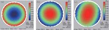
It is shown that before stage II of GaN growth, the interference fringes of reflectivity mapping are almost intact. The maximum reflectivity intensity near the wafer edge reaches earlier (Δ t) than that near the center, meaning phase advance. It is seen that the interference fringes are concave to the left. This means that the growth rate near the edge is faster than that around the center. Since lower wafer temperature leads to faster growth rate at high growth temperature of GaN growth, [28– 30] this difference of growth rate between the edge and the center is due to the slightly concave wafer bow, which is reflected by sample A, as shown in Fig. 4(a). However, during stage II of GaN growth, the wafer bow changes to convex gradually, due to the accumulated compressive stress. As a result, the large convex wafer bow scatters the laser light and leads to the decrease of reflectivity intensity, especially near the wafer edge. Therefore, the interference fringes of the reflectivity mapping are incomplete, namely a deficiency of the interference fringes. The growth rate of GaN at stage II (1.84 μ m/h) is faster than that at stage I (1.73 μ m/h), due to the lower temperature at the center caused by the convex wafer bow during stage II. In addition, the interference fringes are concave to the right, because the growth rate around the center is faster than that near the edge when the wafer bow is convex. After growth, the wafer bow is as large as 188 μ m convex, which was measured by the wafer bow mapping measurement, as shown in Fig. 4(b). This result is in good agreement with the work of Dadgar et al., [31] in which the in-situ curvature measurement was used.
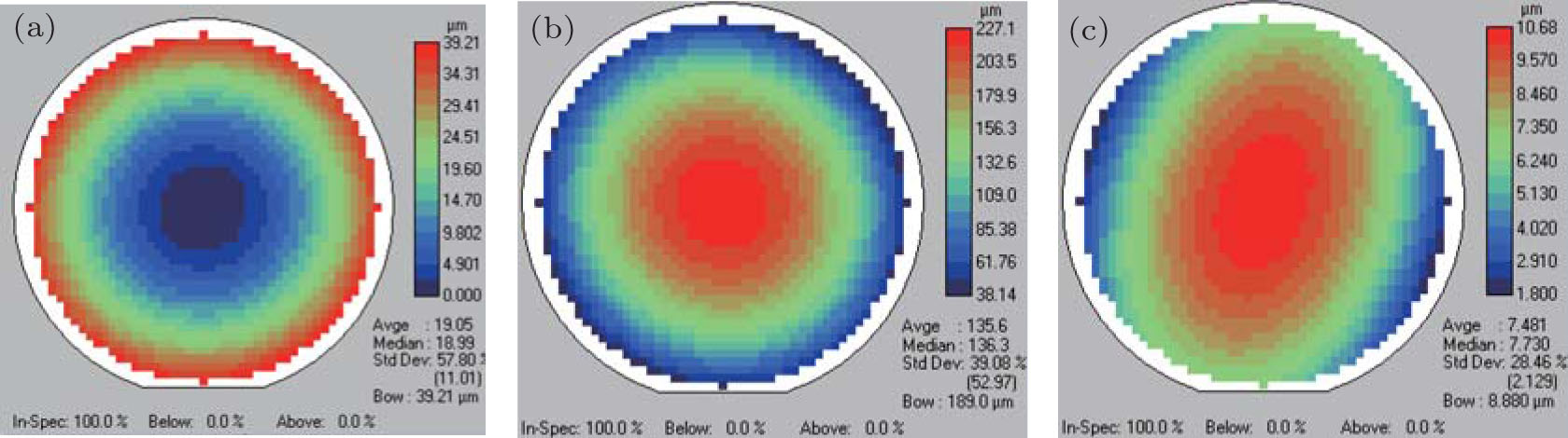
Fig. 4. Wafer bowing images measured by ex-situ method, (a) sample A (bowing: 39.21 μ m, concave), (b) sample B (bowing: 189 μ m, convex), and (c) sample C (bowing: 8.88 μ m, convex).
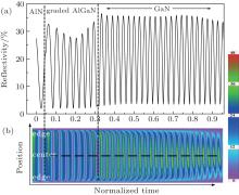
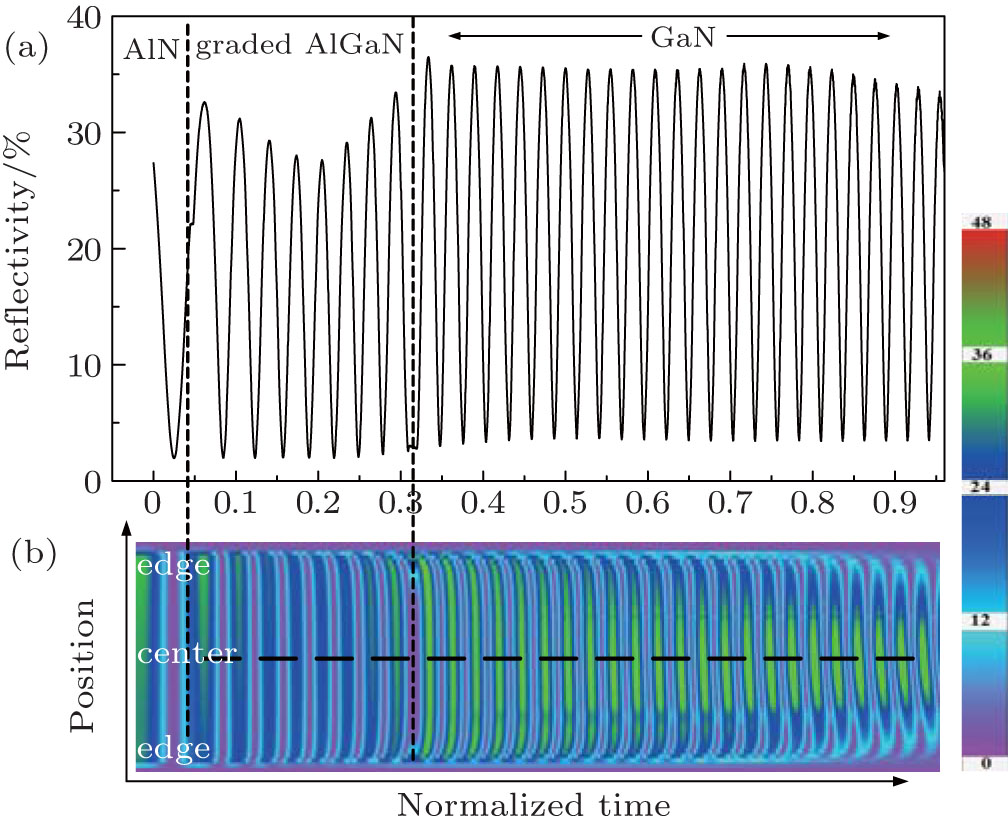
As shown in Fig. 5 for sample C on low-resistivity Si substrate, in the reflectivity mapping, the interference fringes become a little concave to the right at the end of the GaN growth, and the deficiency of the interference fringes is not severe, which indicates a transition to a slightly convex wafer bowing. After the growth process, the wafer bowing is only 8.88-μ m convex (see Fig. 4(c)), corresponding to the observation in the reflectivity mapping. Hence, without the reflectivity mapping, it is difficult to measure the wafer bowing during the growth only with the reflectivity at the center position of the wafer.
Fig. 5. Images of the center position reflectivity (a) and reflectivity mapping (b) for sample C.
4. Conclusions
In this work, we use the reflectivity mapping method to in-situ measure the wafer bowing during growth, which is usually applied to monitor the film thickness and growth rate. The wafer bowing caused by stresses (tensile and compressive) during the epitaxial growth leads to a temperature variation at different positions on the wafer, and the lower growth temperature leads to a faster growth rate and vice versa. Therefore, the wafer bowing can be measured by analyzing the discrepancy of growth rates at different positions on the wafer. That is to say, in the reflectivity mapping, the change of interference fringes demonstrates the transition of wafer bowing. The results are confirmed by the ex-situ wafer bowing measurement. In comparison with high-resistivity Si substrate, GaN grown on low-resistivity substrate shows a smaller wafer bowing. It also can be in-situ measured by using this reflectivity mapping method. Although it is qualitative, the reflectivity mapping method can yet be regarded as a good method to measure the wafer bowing in-situ, due to the lack of an expensive LayTec’ sEpiCurve Sensor. Thus, with the help of the reflectivity mapping method, we may optimize growth parameters and insert interlayers to eliminate the plastic deformation of high-resistivity Si substrate, which will be researched in our later work.
... [1] In order to counterbalance the tensile stress, many solutions have been researched such as low-temperature AlN (LT-AlN) interlayer,[2#cod#x2013 ...
1
2003
0.0
0.0
... [1] In order to counterbalance the tensile stress, many solutions have been researched such as low-temperature AlN (LT-AlN) interlayer,[2#cod#x2013 ...
... [17] Therefore, in-situ techniques play important roles during the growth process, which observes the stress evolution affected by the growth parameters ...
1
2012
0.0
0.0
1
2005
0.0
0.0
... 19] etc ...
1
2012
0.0
0.0
... [20#cod#x2013 ...
1
2007
0.0
0.0
1
2007
0.0
0.0
1
2006
0.0
0.0
1
2004
0.0
0.0
1
2002
0.0
0.0
1
2003
0.0
0.0
1
2004
0.0
0.0
... 27] ...
2
2002
0.0
0.0
... [28#cod#x2013 ...
... Since lower wafer temperature leads to faster growth rate at high growth temperature of GaN growth,[28#cod#x2013 ...
1
2005
0.0
0.0
2
2009
0.0
0.0
... 30] Therefore, the wafer bowing can be measured by analyzing the discrepancy of growth rates at different positions on the wafer ...
... 30] this difference of growth rate between the edge and the center is due to the slightly concave wafer bow, which is reflected by sample A, as shown in Fig ...
2
2013
0.0
0.0
... ,[31] in which the in-situ curvature measurement was used ...
... ,[31] in which the in-situ curvature measurement was used ...
In-situ wafer bowing measurements of GaN grown on Si (111) substrate by reflectivity mapping in metal organic chemical vapor deposition system
[Yang Yi-Bina),b), Liu Ming-Ganga),b), Chen Wei-Jiea),b), Han Xiao-Biaoa),b), Chen Jiea),b), Lin Xiu-Qia),b), Lin Jia-Lia),b), Luo Huia),b), Liao Qianga),b), Zang Wen-Jiea),b), Chen Yin-Songa),b), Qiu Yun-Linga),b), Wu Zhi-Shenga),b), Liu Yang†a),b), Zhang Bai-Jun‡a),b)]


 , Zhang Bai-Jun‡