In-situ wafer bowing measurements of GaN grown on Si (111) substrate by reflectivity mapping in metal organic chemical vapor deposition system

In-situ wafer bowing measurements of GaN grown on Si (111) substrate by reflectivity mapping in metal organic chemical vapor deposition system |
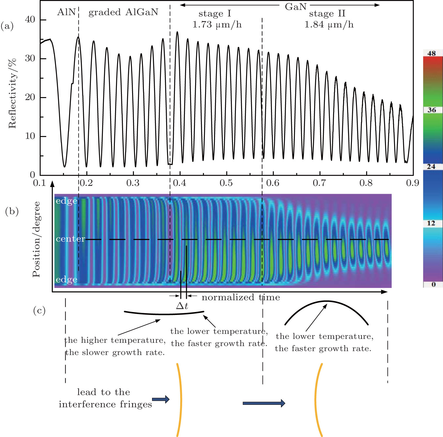
| Reflectivity (a), reflectivity mapping (b), and schematic diagrams (c) of the wafer bow and interference fringes changing of sample B. The reflectivity, which is usually used to calculate the film thickness and growth rate, is equivalent to the dash line at the center position in the reflectivity mapping. |
 |