†Corresponding author. E-mail: jiehuang@swu.edu.cn
‡Corresponding author. E-mail: eeliming@sina.com
*Project supported by the Young Scientists Fund of the National Natural Science Foundation of China (Grant No. 61401373), the Fundamental Research Funds for Central University, China (Grant Nos. XDJK2013B004 and 2362014XK13), and the Chongqing Natural Science Foundation, China (Grant No. cstc2014jcyjA40038).
In this work, a hetero-epitaxial Al0.49In0.51As/Ga0.47In0.53As metamorphic high electron mobility transistor (mHEMT) grown by metal–organic chemical vapor deposition (MOCVD) on p-type silicon substrate has been successfully demonstrated. A novel AlGaAs/AlAs period multiple quantum well (MQW) composite buffer scheme is developed to effectively tune the leakage current from the buffer layer. The quantized room-temperature Hall mobility of the two-dimensional electron gas (2DEG) is larger than 7800 cm2/V·s, with an average sheet carrier density of 4.6×1012 cm− 2. Two-stage electron beam (EB) lithography technology by a JBX-6300 e-beam lithography system is developed to realize a 0.13-μm mHEMT device on Si substrate. A maximum transconductance Gm of up to 854 mS/mm is achieved, and is comparable to that of mHEMT technology on GaAs substrate with the same dimension. The fT and fmax are 135 GHz and 120 GHz, respectively.
As Si-based complementary metal– oxide semiconductor (CMOS) scaling is approaching to the limit of Moore’ s Law, the urgency to explore a new alternative to the conventional Si devices is increasing. Over the past decade, III– V materials have received active and continuous attention as channel alternatives for an n-field effect transistor (n-FET) in future CMOS technology. GaInAs as a channel material closely matches InP, and has shown tremendous potential due to its high electron mobility and low power operations.[1] Recently, AlInAs/GaInAs high electron mobility transistor (HEMT) on Si substrate, which effectively takes advantage of the high carrier drift velocity of GaInAs channel HEMT and the large wafer size and mechanical strength of Si substrate, has been expected to be the most promising device for high-speed and low-power digital logic applications.[2, 3] A seamless, robust heterogeneous integration of high-performance GaInAs mHEMT on Si substrate will enable low-voltage, high-speed III– V-based logic circuit blocks to be combined with the main stream Si CMOS technologies for microprocessor applications in the foreseeable future. To combine the superior carrier transport properties of III– V compounds with Si technologies, one straightforward wafer-level solution directly heteroepitaxially deposits good-quality III– V materials on silicon substrates for device applications. Several different technologies are used in most of the recent studies, such as MBE and MOCVD, to develop AlInAs/GaInAs mHEMTs on the same epi-wafer. However, they still have major technological challenges to be overcome, including the high-density threading dislocation defects in the epi-layers resulting from the large lattice mismatch and the differences in the thermal expansion coefficient between the Si and grown III– V compounds.[4– 7] In 2008, Lau et al. were the first to report and demonstrate metamorphic layer structures grown on Si substrates by MOCVD.[2] However, the device suffered relatively large gate leakage current from the Ge intermediate layer or composition grading buffer layers.
In this paper, in order to reduce the leakage current and improve the comprehensive DC and RF characteristics, a combination of expitial composite buffer growth technology of AlGaAs/AlAs MQW and two-stage EB lithography technology is developed to realize a 130-nm AlInAs/GaInAs mHEMT on Si substrate. The unique composite buffer layer of an AlGaAs/AlAs MQW for the transition from Si to the active device layer is developed to optimize the quality of the heterostructure material and to improve the DC and RF performances. The surface morphology and threading dislocation defects of mHEMT during the epitaxial growth by MOCVD are analyzed in detail. Finally, the devices of 130-nm gate-length mHEMT with a novel, less than 2-μ m metamorphic buffer layer are fabricated and comprehensive DC and RF device characteristics are reported.
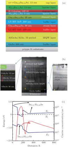
The Al0.49In0.51As/Ga0.47In0.53As mHEMT is grown on a 4-inch (001) oriented p-type silicon substrate by MOCVD (1 inch, = , 2.54 cm). From top to bottom in Fig. 1(a), the Al0.49In0.51As/Ga0.47In0.53As mHEMT consists of a 13-nm Ga0.47In0.53As cap layer heavily doped with Si (7× 1018 cm − 3, 13-nm undoped Al0.49In0.51As Schottky barrier layer, Si-delta-doping layer (6× 1012 cm − 3, 5-nm undoped Al0.49In0.51As spacer layer, 30-nm Ga0.47In0.53As channel, and a 2.0-μ m composite buffer stack. From bottom to top, the 2.0-μ m composite buffer stack includes 300-nm GaAs nucleation layeSSr, 10-period AlGaAs/AlAs MQW layers (1 μ m), 300-nm low temperature (HT)/high temperature (HT) GaAs buffer layer, 30-nm Ga0.47In0.53As strain balance layer, and 300-nm composite LT/HT InP-lattice-matched AlInAs buffer layer grown at 500 ° C/600 ° C. The corresponding epitaxial structure schematic diagram is shown in Fig. 1(a). The 10-period AlGaAs/AlAs MQW (1 μ m) is introduced into the HT-GaAs buffer layer to further prevent the defection or dislocation from penetrating into the top InP-matched layer. The thickness of the composite buffer is successfully scaled down to 2 μ m for the first time. High-resolution triple-axis x-ray diffraction (HRXRD) is used to monitor the composition and relaxation state of these layers. The measured full-width at half maximum (FWHM) values of the GaAs buffer and InP buffer are around 328 arcsec and 320.3 arcsec, respectively, which indicates a good crystalline quality that is desirable for the good device performance.
A cross-sectional TEM image of the mHEMT grown on Si substrate with composite buffer is shown in Fig. 1(b), where few misfit dislocations and 60-degree threading dislocations could be observed in the composite buffer. The actual thickness of each layer is consistent with the designed thickness. The 300-nm thick AlInAs buffer, which includes LT and HT grown layers, is grown as a high resistivity isolation layer. A comparatively low defect density exists in the HT-AlInAs buffer due to the insert of LT-AlInAs layer, which has a thickness of at least 150 nm as an effective buffer to effectively prevent the threading dislocations. The simulated band diagram and corresponding electron distribution of Al0.49In0.51As/Ga0.47In0.53As mHEMT with a quantum well structure is illustrated in Fig. 1(c). The excellent characteristic of distribution of channel carries and crystalline quality guarantee the development of high-performance GaInAs mHEMT on silicon substrate.
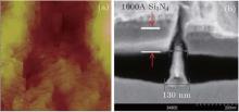
An atomic force microscopy (AFM) image of an Al0.49In0.51As/Ga0.47In0.53As mHEMT structure across a scanned area of 5 μ m× 5 μ m is shown in Fig. 2(a). The root mean square (RMS) value of surface roughness of 2.4 nm is measured. Compared with Lau et al.’ s work, [2] a smoother surface is demonstrated. In order to characterize the quality of the 2D electron gas (DEG), the Van Der Pauw– Hall measurements are carried out at 300 K and 77 K. The measured electron mobilities of 7800 cm2/V· s and 23000 cm2/V· s are obtained at 300 K and 77 K, with corresponding sheet carrier densities of 5× 1012 cm − 2 and 3× 1012 cm − 2, respectively. The mobility of 2DEG at 77 K is greatly enhanced, and these mobility values are somewhat comparable to that of similar structure grown on GaAs substrate by MOCVD.[8, 9] The excellent mobility performance of AlInAs/GaInAs mHEMT on Si substrate is attributed to the smoother InP-lattice-matched AlInAs buffer layer and AlGaAs/AlAs MQW composite buffer layer.
 | Fig. 2. (a) AFM image of a typical mHEMT structure, and (b) TEM cross-section micrograph of T-shaped gate |
Two-stage electron beam (EB) lithography technology by a JBX-6300 e-beam lithography system is developed to fabricate a 130-nm AlInAs/GaInAs mHEMT on Si substrate. Firstly, AlInAs/GaInAs mHEMT is isolated by wet chemical etching, followed by source/drain definition. Then, the Ohmic metallization is achieved by the electron beam evaporation of Ni/Ge/Au/Ge/Ni/Au and lift-off process. At the same time, the measurement of contact resistivity is performed by transmission line model (TLM) method, a typical result is 0.06 Ω · mm. Secondly, first-stage EB lithography is used to determine the gate-footprint of T-shaped gate. The 100-nm SiNx layer is deposited, followed by coating ZEP520 electron beam (EB) resist. ZEP520 EB resist is exposed at 1000 μ c/cm2 and is then developed in ZEN-N50 for 5 s. Then, SiNx film is etched by CHF3/CF4/O2 reactive ion etching (RIE) to mechanically support the T-shaped gate. The second-stage EB lithography is employed to form the gate-head pattern by coating bilayer polymethylmethacrylate/polymethylglutarimide (PMMA/PMGI) EB resist, followed by the EB exposition and selective development.[10, 11] Thirdly, the gate-recess etching is performed by the use of Succinic-based acid to remove the highly doped GaInAs cap layer, followed by gate metallization through evaporating Ti/Pt/Au on the AlInAs barrier layer and lifting off. Finally, the electrodes of the mHEMT device were formed by the e-beam evaporation of Ti/Au and the lift-off process for the AlInAs/GaInAs mHEMT. A SEM cross-sectional photograph of T-shaped gate with 130-nm gate-length and 400-nm head-widths is shown in Fig. 2(b).
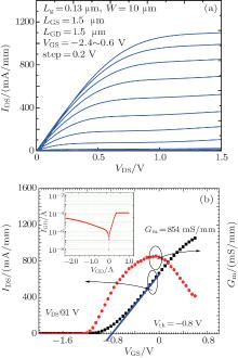
The measured current– voltage output characteristics of 0.13 μ m× 100 μ m AlInAs/GaInAs mHEMT on Si substrate at room temperature by HP 4155 semiconductor parameter analyzer are shown in Fig. 3(a), where the gate– source voltage VGS increases from (bottom) − 2.4 V to (top) 0.6 V in step of 0.2 V. The maximum drain current (IDS, max) of 1.13 A/mm is obtained at VGS= 0.6 V and VDS= 2 V, and is a new record of GaAs mHEMT on Si substrate. The peak extrinsic transconductance (Gm, max) of 854 mS/mm is obtained at the gate bias VGS= − 0.15 V and the drain bias VDS= 1.5 V as shown in Fig. 3(b). The threshold voltage (Vth) of − 0.8 V is derived by a linear extrapolation from the transfer curve shown in Fig. 3(b) at VDS= 1 V, and indicates that the device is a depletion-mode transistor. The drain current after pinch-off is less than 1.8 mA/mm at VGS = − 2.0 V and VDS = 1.0 V. The leakage current characteristic of the gate Schottky barrier of the mHEMT on Si substrate is shown in the inset of Fig. 3(b), where a slightly high reverse gate leakage current is due to the lack of passivation and a relatively high Schottky barrier height of 0.4 V is determined as the gate voltage when gate current is 0.1 mA. The gate leakage characteristic can be further improved by optimizing the structure of MQW composite buffer and InP-lattice-matched AlInAs buffer, which will be performed in future.
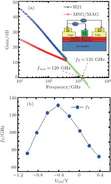
The RF performance of 0.13 μ m× 100 μ m AlInAs/GaInAs mHEMT on Si substrate is obtained from the S-parameter measurements in a frequency range from 0.1 GHz to 39.1 GHz by Cascade Microtech probes and an HP8722 network analyzer at room temperature. The network analyzer is calibrated using an off-wafer standard short-open-load-through calibration, and on-wafer open and short patterns are used to de-embed the parasitic capacitances and inductances of the probe pads from the measured S-parameters of the mHEMT. Figure 4(a) shows the current gain | h21| 2 and the maximum stable gain (MSG)/maximum available power gain (MAG) from the measured S-parameters after de-embedding as a function of frequency under the peak fT bias condition VGS = − 0.4 V and VDS= 1.0 V. The current cutoff frequency fT is estimated to be 135 GHz from the extrapolation of | h21| 2 with − 20 dB/decade line, and the maximum frequency of oscillation fmax of 120 GHz is extrapolated by the − 20 dB/decade slope in MSG/MAG curve. To the best of our knowledge, fT of 135 GHz is the highest ever reported for AlInAs/GaInAs mHEMT on Si substrate by MOCVD featuring the same gate-length. The dependence of fT on the gate bias is shown in Fig. 4(b), where fT is symmetrical about gate voltage VGS and demonstrates a good linearity with VGS at both low and high gate biases.
The relationship between fmax and fT is characterized by Eq. (1), [11] and is determined by the source resistance Rs, gate resistance Rg, drain conductance Gds, intrinsic transconductance Gm, capacitance ratio Cgs/Cgd between the input gate-source capacitance and the feed-back gate– drain capacitance, and voltage gain Gm/Gds. Table 1 shows the extracted equivalent circuit model parameter values from the measured 10 GHz– 30 GHz S-parameters at VGS = − 0.1 V and VDS = 1.0 V. Especially, to a great extent, the value of fmax largely depends on the capacitance ratio Cgs/Cgd and voltage gain Gm/Gds. The relatively low output conductance (Gds) of 14.8 mS and Gm/Gds of 7.2 are successfully obtained. Moreover, the capacitance ratio Cgs/Cgd of 2.4, which is mainly responsible for the degradation of fmax in our mHEMT, leads to the high fmax of 120 GHz.

| Table 1. Small-signal equivalent circuit model parameters of 130-nm mHEMTs. |
Table 2 shows a comparison of mobility (μ ), Gm, fT, and fmax for the recently reported AlInAs/GaInAs HEMTs, which are grown by MBE or MOCVD on GaAs or InP or Si substrates. The DC performance of mHEMTs grown by MOCVD is comparable to those of HEMTs by MBE. The metamorphic growth technology is used to manufacture mHEMTs on Si substrates in this work, and therefore more dislocations and rougher surface are inevitably introduced in the active layers than lattice-matched ones on InP substrates. However, they still exhibit attractive RF characteristics, which are very encouraging to the manufacture of metamorphic HEMTs on Si substrates by MOCVD for high-speed and low-power digital logic applications in the future.
| Table 2. Comparison of performance among AlInAs/GaInAs HEMTs. |
In this work, metamorphic AlInAs/GaInAs HEMTs on silicon substrates grown by MOCVD have been successfully fabricated by two-stage EB lithography technology and MQW composite buffer growth technology. In these high-quality Ga0.47In0.53As structures, the novel metamorphic buffer layer developed has a length of less than 2 μ m, which effectively accommodates the lattice mismatch between the mHEMT device and the silicon substrate, thereby leading to a high-performance mHEMT with a relatively small gate leakage current. A 130-nm gate-length depletion-mode mHEMT exhibits a saturated peak DC transconductance of 854 mS/mm and an intrinsic fT of 135 GHz at VDS= 1.0 V and VGS = − 0.1 V. These encouraging results show the possibility of integrating the high-speed and low-power AlInAs/GaInAs mHEMT with the large-size and strong-mechanical-strength Si substrate for ultra-high-speed logic digital applications. The technology of mHEMT on silicon substrate by MOCVD that we have developed is very attractive for manufacturing low cost, large-scale similar CMOS ICs.
| 1 |
|
| 2 |
|
| 3 |
|
| 4 |
|
| 5 |
|
| 6 |
|
| 7 |
|
| 8 |
|
| 9 |
|
| 10 |
|
| 11 |
|
| 12 |
|
| 13 |
|
| 14 |
|


