Hetero-epitaxy of Lg = 0.13-μm metamorphic AlInAs/GaInAs HEMT on Si substrates by MOCVD for logic applications

Hetero-epitaxy of Lg = 0.13-μm metamorphic AlInAs/GaInAs HEMT on Si substrates by MOCVD for logic applications |
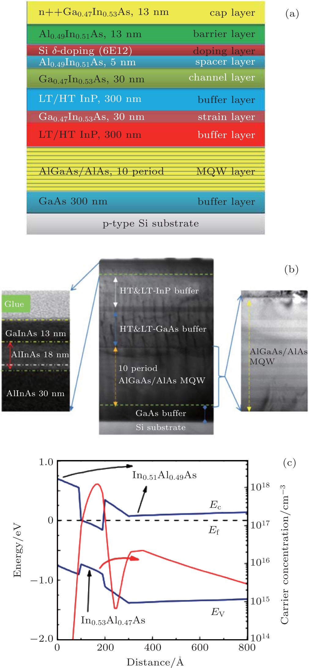
| (a) Nominal structure of mHEMT device on Si substrate, (b) TEM cross-section micrograph of mHEMT structure (note: panels (a) and (b) are not drawn to scale), (c) simulated band diagram and electron distribution of the mHEMT with quantum well structure. |
 |