


Progress in bulk GaN growth*
[Xu Kea), b)†  , Wang Jian-Feng
a), b) , Ren Guo-Qianga), b) ]
, Wang Jian-Feng|
|


†Corresponding author. E-mail: kxu2006@sinano.ac.cn
*Project supported by the National Natural Science Foundation of China (Grant Nos. 61325022 and 11435010), the National Basic Research Program of China (Grant No. 2012CB619305), and the National High Technology Research and Development Program of China (Grant No. 2014AA03260).
Three main technologies for bulk GaN growth, i.e., hydride vapor phase epitaxy (HVPE), Na-flux method, and ammonothermal method, are discussed. We report our recent work in HVPE growth of GaN substrate, including dislocation reduction, strain control, separation, and doping of GaN film. The growth mechanisms of GaN by Na-flux and ammonothermal methods are compared with those of HVPE. The mechanical behaviors of dislocation in bulk GaN are investigated through nano-indentation and high-space resolution surface photo-voltage spectroscopy. In the last part, the progress in growing some devices on GaN substrate by homo-epitaxy is introduced.
III-nitride semiconductors, including GaN, AlN, InN and its alloys, have a direct band gap ranging from 0.65 eV to 6.2 eV, covering the deep ultraviolet, near ultraviolet (UV) and the whole visible light spectrum, play an important roles in the application of solid-state lighting, high-density data storage, displays, solar cells, UV sterilization, UV detection, etc. Beyond that, with their advantages of high breakdown voltage, high saturated electron drift velocity, high thermal conductivity, and strong piezoelectric coefficients, III-nitride semiconductors are also suitable materials for the fabrication of microwave and power devices.[1– 7]
In the past thirty years, the performance of III-nitrides-based devices has developed rapidly from prototype to the commercial application level, which depended on the improvement of crystal quality of GaN-based materials. In 1986, two-step growth was first proposed for the dramatic reduction of dislocation density in GaN films.[8] Combined with the subsequent progress in the realization of p-type GaN, [9] it made both the blue LED and III-nitride solid state lighting[10] possible. The Nobel Prize for Physics of 2014 was awarded for such great progress. Then the epitaxial lateral overgrowth method was transferred from the growth of silicon and GaAs materials to GaN, [11] it helped to further reduce dislocation density in GaN films and realize GaN-based laser diodes.[12]
However, suffering from the big difficulties in crystal growth, the development of GaN bulk substrate seems to be falling behind the wide application of GaN-based devices based on hetero-epitaxy. The decomposition pressure at the melting point is extremely high (∼ 6 GPa), which poses critical difficulties for the traditional melt solidification method in bulk GaN growth with thermal dynamical equilibrium condition. Theoretically, it needs high growth pressure of about 6 GPa and high growth temperature of about 2200 ° C.[13]
Crystal growth technologies are widely developed for the realization of GaN substrate with large size and high quality.[14] There are mainly three routes as given below. The first one is improved from the high-pressure high-temperature growth method. By adding sodium into the Ga melt for the enhancement of N concentration, the sodium flux growth method can grow GaN under a temperature about 800 ° C and lower pressure of 5 MPa.[15] The second route is based upon the hydrothermal method, which is very mature for the growth of quartz. It is called the ammonothermal method. By using ammonia as the solvent, and KNH4 or NH4Cl as mineralizer, GaN crystal can be grown under low temperature of about 600 ° C and high pressure about 400 MPa.[16]
The third growth method is HVPE, which is initially used in the growth of GaAs and InP.[17] With HVPE’ s advantage of high growth rate, i.e., several hundred micrometers per hour, GaN can be grown up to several millimeters, which is thick enough for the fabrication of bulk substrates. However, since GaN seed crystal is hardly available, thick GaN films have to be grown on foreign substrates, such as sapphire, GaAs, and silicon. The big lattice and thermal mismatch between GaN film and the foreign substrate bring big challenges of strain control and dislocation reduction. On the other hand, separation of GaN from the foreign substrate is another challenge after the HVPE growth. Self-separation and laser-lift-off techniques are well developed to obtain crack-free GaN films.
In this paper, the progress of bulk GaN growth is reviewed. In Section 2, the principles of different growth methods are introduced. In Section 3, we focus on the main challenges and solutions of HVPE growth, including dislocation reduction, strain control, separation, and doping of GaN film. In Sections 4 and 5, the progress of Na-flux and ammonothermal growth of GaN substrate is discussed, respectively. In Section 6, the dislocation behavior in GaN film is investigated through nano-indentation and home-made local surface photo-voltage spectroscopy. In Section 7, the progress of some devices grown on GaN substrate by homo-epitaxy is introduced. The final part is the conclusion and outlook in Section 8.
Because the decomposition pressure at the melting point (∼ 2200 ° C) is extremely high (∼ 6 GPa), [18] GaN decomposes under the pressure instead of growing.[15, 16] And the standard techniques of crystal growth (Bridgman, Czochralski) cannot be employed for GaN growth.
Using the direct reaction between gallium and nitrogen, scientists developed the high-pressure nitrogen solution (HPNS) method and Na-flux method for GaN crystal growth.[15, 16] To realize the GaN growth, it is necessary to enhance the N solubility in Ga melt for both of the two methods. The N solubility is relatively high in an HPNS system benefiting from high temperature and high pressure growth conditions. While in the Na flux system, high solubility of N is achieved by adding sodium into gallium melt.
The growth mechanism of HPNS is as follows: Nitrogen molecules dissociate on gallium surface and dissolve in the metal, and then nitrogen atoms transport from the hot region of the solution to the cooler region, and finally GaN crystallizes and grows. Due to the very low solubility of nitrogen in Ga less than 0.5%, the growth rate is very slow, and the crystal sizes have been limited to several millimeters. It is difficult to grow crystals for industrialization due to the slow growth rate and the critical growth conditions. Despite these disadvantages, the HNPS method grows very high-quality “ truly” bulk GaN with dislocation density less than 2 × 102 cm− 2 by spontaneously nucleation.[16]
In the Na-flux method, by adding sodium into Ga melt, the growth temperature and pressure can be greatly decreased to 750 ° C– 900 ° C and 3 MPa– 5 MPa, which are only 50% and 0.3% of the growth conditions used in HPNS, respectively. The basic growth process is as follows: First of all, the nitrogen molecules are ionized by Na at the gas– liquid interface, and the ionized nitrogen is easily dissolved in the Ga– Na melt system. Then the nitrogen atoms combine with gallium atoms or additives (carbon, lithium, etc.). When the N concentration exceeds the critical growth concentration in the system, spontaneous nucleation of GaN crystal takes place. On the other hand, forming complex compounds, the nitrogen atoms could be transported to the surface of the GaN seed; generally the GaN seed was grown by MOCVD or HVPE method. As time goes on, most N atoms will contribute to the GaN seed in the bottom of a crucible. When the N concentration exceeds the critical growth concentration, Liquid Phase Epitaxy (LPE) will happen.[19] Normally, high super-saturation generated by increased nitrogen concentration would grow transparent GaN single crystal at a fast growth rate. In summary, in order to obtain high quality GaN crystal by the Na-flux method, one way is to grow GaN crystal by spontaneous nucleation, and the other way is to grow GaN crystal by LPE.
Inspired by mass production of quartz grown by the hydrothermal method, the ammonothermal method was developed for GaN crystal growth. The ammonothermal process is analogous to the hydrothermal method, which allows solubilization of polycrystalline GaN nutrient or feedstock in supercritical ammonia under high pressure. The process of ammonothermal growth is as follows: The autoclave is divided into growth zone (lower solubility of GaN) and feeding zone (higher solubility of GaN) by a baffle through the temperature gradient control. By convection, dissolved GaN nutrient with higher solubility is transported to the growth zone from the feeding zone, and GaN crystallizes and grows on the seeds due to the supersaturation in the growth zone. And the remaining dissolved nutrient is transmitted to the feeding zone in the role of convection, which is unsaturated relative to the solubility of feeding zone. Therefore, the GaN nutrient continues to dissolve. Thus, a gallium nitride growth cycle is realized.[20]
However, the solubility of GaN in supercritical ammonia remains in insufficiency for ammonothermal growth. And mineralizers are used to increase the solubility of nutrients. The mineralizers commonly used at present can be divided into two typical types: basic mineralizers, such as MNH2 (M = Na, Li, K), and acidic mineralizers, such as NH4X (X = Cl, Br, I). As a consequence of different chemical nature, basic mineralizers and acidic mineralizers of the ammonothermal technique are different: the coefficient of the solubility is positive in the ammonoacidic solutions, while negative in the ammonobasic solutions.[21]
Generally, an HVPE reactor for GaN mainly includes two reacting zones. One is the source zone for providing chloride gas of gallium and the other is the deposition zone, in which the GaN is formed from the reaction of gallium source and nitride source (NH3). Therefore, in HVPE growth, the main chemical reactions can be divided into two parts. One is in the source zone where the gallium is kept at a certain temperature and reacts with HCl gas, which is commonly used as reactive gas and introduced into the source zone over metal to form chloride gas of gallium. Then the gaseous species formed at the source zone are transported by carrier gas to the deposition zone for further react with nitride source to form GaN. The carrier gases are generally H2 and inert gas (N2, He, Ar, etc.).
In the source zone, the gaseous species and their equilibrium partial pressures are very important for the formation of GaN in the deposition zone. Generally, the chemical reactions simultaneously happen in the source zone:


The equilibrium partial pressures in the source zone can be calculated by thermodynamic analysis.[22] In HVPE growth, the temperature of the source zone is usually around 850 ° C, at which the major gaseous species of gallium is formed by Eq. (1). It should be noticed that the input partial pressure of HCl should not be too high in order to make almost all the HCl introduced into the source zone react with gallium. Therefore, the equilibrium partial pressure of GaCl should be almost equal to that of HCl at the source zone. From the thermodynamic analysis, if the temperature of the source zone is too low or the partial pressure of input HCl is too high, or the reaction area of gallium with HCl is too small, the reactions might be insufficient in the source zone, which means the reactions will be kinetically limited.
The GaCl formed at source zone and NH3 are transported to the deposition zone separately by a carrier gas mixture of H2 and inert gas. At the deposition zone, the source species are mixed and the following chemical reactions occur simultaneously


Then, gaseous species at the growth zone include GaCl, GaCl2, GaCl3, (GaCl3)2, NH3, HCl, H2, and inert gas. The partial pressures of these gaseous species at the growth zone as a function of temperature at deposition zone have been calculated by Koukitu et al.[23] The partial pressures of (GaCl3)2 and GaCl2 are very small under typical growth conditions. The equilibrium constants for these reactions can be calculated from the equilibrium equations.[24] GaCl3 also reacts with NH3 to form GaN, whose equilibrium constant is close to zero at the usual growth temperature. Though the equilibrium constants are close for both reactions using GaCl and GaCl3, the partial pressure of GaCl3 is far lower than that of GaCl. Therefore, equation (5) is the dominant reaction.
The driving force for the deposition can be obtained from the difference between the number of Ga atoms put in and the amount of Ga atoms remaining in the vapor phase, which can be written as[23]

where 
In contrast to classical semiconductors like Si and gallium arsenide (GaAs), for which device structure is based on high quality native substrate with low cost, the GaN-based device technology is far more advanced than that of native GaN substrate crystal growth. Many scientists and engineers are working hard to change this situation and have made great progress with different methods of GaN crystals in recent years. The following table lists the contrast of growth conditions and progress for different bulk GaN growth methods.
| Table 1. The contrast of growth conditions and progress for different bulk GaN growth methods. The unit: 1 atm = 1.01325 × 10⁵ Pa, 1 inch = 2.54 cm. |
To obtain high quality and crack-free bulk GaN substrate, dislocation reduction and strain control are the most important issues during HVPE growth. Epitaxial lateral overgrowth (ELOG) is an effective and traditional method to bend the dislocation line and form void-structure in GaN films simultaneously, which helps to enhance the dislocation annihilation for dislocation reduction and helps to release the growth and thermal stress.[28, 29]
A standard ELOG process is as follows: (i) Depositing mask film such as SiN, SiO2, etc. on GaN film; (ii) Etching dielectric film to expose GaN as window area; (iii) GaN layer grows from the window and then laterally overgrows to cover the mask. By carefully adjusting the mask/window shape and the growth parameters for the overgrowth, reasonable lateral overgrowth rate and smooth surface can be achieved.[28, 30– 32] Other technologies based on ELO have been proposed, like double-layer ELO[33, 34] and three-step ELO, [35] in order to eliminate the remaining threading dislocations (TDs) in the coalescence region.
By improvement of ELOG technology, some special technologies have been developed in HVPE system for the growth of high quality and crack-free GaN layers, such as dislocation elimination by epitaxial growth with inverse-pyramidal pits (DEEP), TiN-based nano-mask and photoelectron-chemical etched nanowires.
DEEP was reported by Kensaku Motoki from Sumitomo Electric.[36] During the growth of the GaN layer, there are numerous large hexagonal inverse-pyramidal pits constructed mainly by {11-22} facets appearing on the surface. While GaN grows, dislocations are collected to the center of the hexagonal pits parallel to (0001) in the ⟨ 11-20⟩ or ⟨ 1-100⟩ direction, and therefore dislocations are eliminated within the hexagonal pits except for its center. The DEEP method can produce a high quality GaN layer, but the dislocation distribution on the surface of GaN is not uniform. Far from the center of a pit, dislocations are few; in contrast, the center of a pit gathering dislocations possesses very high dislocation density (DD).[37, 38]
Besides ELOG and DEEP, nano-mask is recognized as a good approach that not only reduces the DD but also easily separating the freestanding GaN from sapphire. Yuichi Oshima et al. developed a novel technique for preparing large-scale freestanding GaN wafers called VAS (void-assisted separation) by thin TiN film.[39]
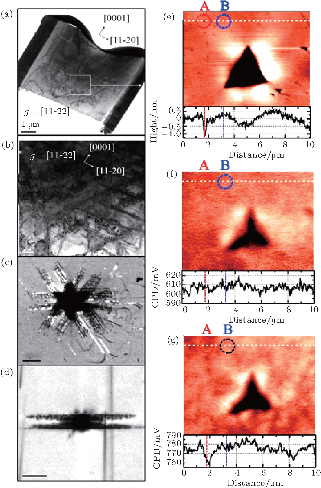
ELOG, DEEP, and nano-mask all use dielectric film as the mask for the overgrowth of GaN. Another unique method without dielectric film as mask was developed in our Institute.[40] By electrode-less photoelectron-chemical (PEC) etching, long and straight GaN nanowire arrays are obtained, which have a density about 107 cm− 2, with diameters ranging from 150 nm to 500 nm, and corresponding lengths ranging from 10 μ m to 20 μ m. It is found that the GaN nanowires (NWs) are almost dislocation- and strain-free (Figs. 1(a) and 1(b)), because PEC etching begins from the dislocation core. Based on these GaN NWs, we can get high-quality and crack-free GaN layer (Figs. 1(c) and 1(d)), with thickness about 400 μ m and dislocation density about 104 cm− 2– 106 cm− 2.
 | Fig. 1. (a) SEM image of GaN NW array, [40] (b) weak beam dark-field TEM image with g = 11-22, revealing that the GaN NW does not possess dislocations, [40] (c) photo of a 400-μ m GaN based on the PEC GaN NW arrays template, (d) panchromatic CL image shows that the DD of panel (a) is 3 × 106 cm− 2. |
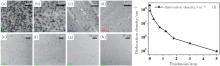
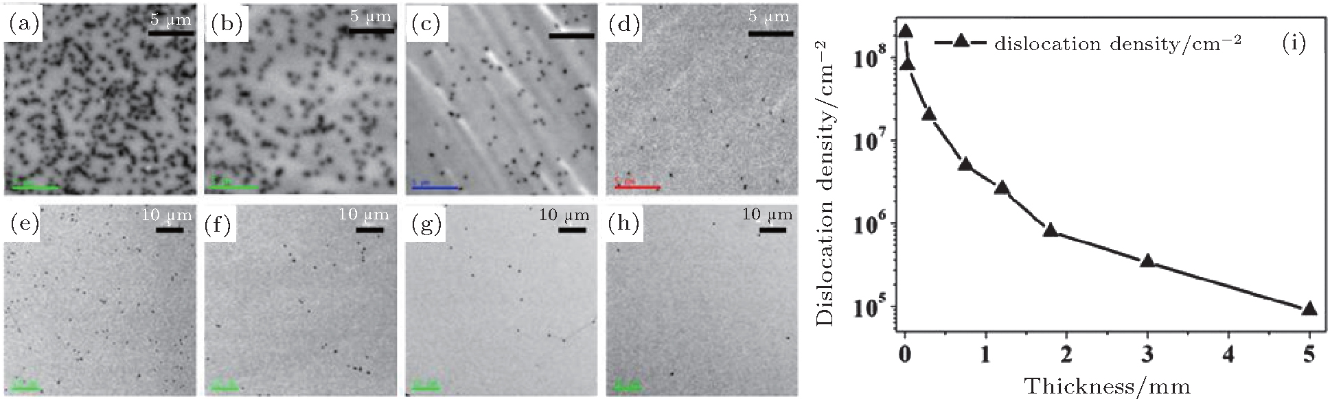 | Fig. 2. Thickness from 5 μ m to 5 mm and panchromatic CL images: (a) 5 μ m, 2 × 108 cm− 2; (b) 20 μ m, 5 × 107 cm− 2; (c) 200 μ m, 2 × 107 cm− 2; (d) 0.7 mm, 5 × 106 cm− 2; (e) 1.2 mm, 3 × 106 cm− 2; (f) 1.8 mm, 8 × 105 cm− 2; (g) 3 mm, 3.4 × 105 cm− 2; (h) 5 mm, 8.0 × 104 cm− 2; (i) the relation between thickness and DD. |
In addition to the above mentioned methods, increasing the thickness of GaN is another effective approach to decrease the defect density of GaN substrate. The dislocation density reduced to 106 cm− 2 as the thickness increased to 5 mm.[41] According the same research from our group, it is found that the dislocation density declines sharply from 108 cm− 2 to 104 cm− 2 when the thickness increases from several micrometers to several millimeters (Figs. 2(a)– 2(h)). The related panchromatic CL images of different thickness GaN are shown in Fig. 2.
A novel technique for separating large-diameter GaN wafers from sapphire is self-separation technology, mainly based on the void-assisted separation process.[42– 49] The critical factors of void-assisted separation include the choice of mask material and the optimization of geometry and density (fill factor) of the mask. Oshima et al.[43] used a TiN nano-net structure by annealing the 20-nm thick Ti layer and succeeded to separate the 300-μ m thick GaN from the sapphire by controlling the partial pressure of H2 in order to control the fill factor. Three-inch crack-free FS-GaN wafers were successfully fabricated by this method.[44] Another useful mask material was pure SiN or SiN with a high fraction of tungsten (WSiN), by adjusting the fill factor of the mask, 2-inch crack-free FS-GaN wafers can be separated from the sapphire.[45, 46] Other void-assisted separation processes, such as Ni mask with nano imprint lithography method[47] and growth of a voids- or pit-inducing GaN buffer layer, [48, 49] were also introduced to successfully fabricate 2-inch and nearly 4-inch FS-GaN wafers.
A new simple self-separation method was delamination of the inside GaN layer by heat treatment of sapphire, [50] but there was 80 μ m– 150 μ m residual GaN on separated sapphire. All of the above-mentioned self-separation technology may have the disadvantage of low reproducibility to obtain crack-free, large-diameter FS-GaN wafers.
Another method to obtain the FS-GaN wafers is laser lift-off (LLO) technology.[51, 52] A typical schematic view of the LLO process is shown in Fig. 3(a). An ultraviolet laser with the photons energy higher than the bandgap energy of GaN (∼ 3.45 eV) and less than that of sapphire (∼ 9.9 eV) can be used to decompose the interfacial GaN layer into metallic Ga and gaseous N2, e.g. the 248 nm (5 eV) KrF excimer laser[51] and 355 nm (3.49 eV) Nd:YAG laser.[52] The main difference in influence of the two lasers on the LLO of GaN is the threshold energy density and decomposed thickness of GaN.[53] Typical threshold energy of the KF excimer laser is about 600 mJ/cm− 2, because of a typical pulse width of 38 ns, whereas 300 mJ/cm− 2 is sufficient for the Nd:YAG laser, and its typical pulse width is 6 ns.
One critical problem in the LLO process of ∼ 300 μ m thickness GaN wafers is the fracture of the sample caused by thermal stress relaxation. The E2 (high) peak values of GaN/sapphire interface before LLO and N polar of GaN after LLO were 569.3 cm− 1 and 567.8 cm− 1, [54] respectively, indicating that the interface compressive stress was about 0.4 GPa, calculated by the formula according to the conclusions of Kisielowski et al.[55] As a result, a heating plate above 800 ° C was used to release the compressive stress of the sample during the LLO process and avoid fracture.
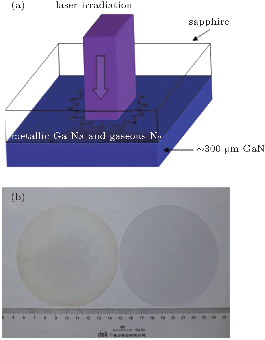 | Fig. 3. (a) Schematic view of the laser lift-off (LLO) process, (b) photograph of the 4-inch FS-GaN wafer and the corresponding sapphire after LLO. |
Another source of cracks in the process of LLO is laser-induced shock waves, causing damage at the N-polar face of GaN. Keeping the shock wave-induced stress under the damage threshold of GaN is effective to avoid crack generation during LLO. Therefore, the effective spot size of 270 μ m ∼ 400 μ m and the ratio of laser spot size to effective spot size of 7.3∼ 11 are the critical parameters for our LLO process, [54] LLO technology is more stable and reproducible technique than the self-separation technology. In our optimized conditions, we can achieve more than 90% yield of crack-free 2-inch ∼ 300-μ m thick FS-GaN wafers now. Furthermore, although 1.5-inch∼ 2-inch FS-GaN wafers fabricated by LLO technology have been reported several times, [52, 56– 58] there are few reports about 4-inch FS-GaN obtained by LLO technology. With the development of our home-made LLO equipment, we demonstrate the separation of 4-inch FS GaN layers from sapphire. A typical photograph of 4-inch FS-GaN wafer and the corresponding sapphire after LLO is shown in Fig. 3(b).
The growth of un-doped GaN is simple but not suitable to make LEDs, LDs or high power electronic devices, because its resistivity is relatively high, with the typical value about 1 Ω · cm. In order to control its electrical properties, flexible and reproducible doping during HVPE growth of GaN is necessary and important.
SiH4 is mostly used as the n-type doping source in MOCVD, [59] but it is not suitable in HVPE, most of which occurs in a hot-wall system with typical growth temperature about 1040 ° C. SiH4 will decompose into silicon and hydrogen before it is transported to the growth zone of the HVPE system, contributing less to the doping process. Great efforts have been made to find a proper doping source. Undoped single crystalline Si was used to react with HCl gas to produce dopants, [60] but it is difficult to realize precise control of the doping level. Dichlorosilane (SiH2Cl2) is a suitable choice[61] for HVPE growth of Si-doped GaN because of its higher thermal stability.
The free carrier concentrations increase linearly in a semilog-plot with SiH2Cl2 flow rates from 5 sccm to 25 sccm.[61] This is different from the case in MOCVD growth of Si-doped GaN with SiH4, where the free carrier concentrations increase linearly with SiH4 flow rates.[59]
The growth rate of GaN in HVPE is tens to hundreds of microns per hour, higher than that in MOCVD, so HVPE could easily realize growth of GaN with different dislocation densities. The influence of dislocation density on electron mobility is carefully studied. It is found that the mobility of FS GaN is higher than that of the GaN template at the same carrier concentration, with the dislocation density about 106 cm− 2 for the freestanding GaN and 108 cm− 2 for the GaN template. Edge dislocation introduces acceptor centers along the dislocation line, which could capture electrons and make the dislocation lines negatively charged. When electrons travel across the dislocations, they will be scattered, thus reducing mobility.[62]
Semi-insulating (SI)-GaN substrate is very important for performance of GaN-based HEMT device. However, un-doped GaN grown by HVPE generally shows n-type conductivity due to residual donor impurities such as O and Si, which may degrade device performance. By compensation of the residual carriers from electron trapping centers, SI crystal is obtained by doping with Fe, Cr, or Zn.[63– 65] Among these different doping elements, Fe-doping is widely used for reproducibility and controllability. An Fe concentration above 1015 cm− 3 is sufficient to compensate unintentionally incorporated donor impurities (oxygen and silicon) and native defects in GaN for the SI property.[66, 67] Although the formation energy and concentration of the point defects and/or the complex structure will be changed during the annealing process, the SI property of GaN:Fe bulk films grown by HVPE is thermally stable up to 1050 ° C.[68] The resistivity decreases with the temperature with an activation energy about 0.5 eV– 0.6 eV, which is attributed to Fe deep acceptors.[66, 69] Fe-doped bulk SI GaN (SI-GaN:Fe) grown by HVPE has been commercialized, resulting in a significant improvement of device performance and reliability of the AlGaN/GaN heterostructure field effect transistors.[70, 71] Besides the SI property, other properties of the GaN:Fe also have gained wide interest, such as a diluted magnetic semiconductor to realize future spintronic applications.[72, 73]
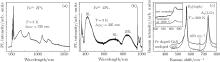
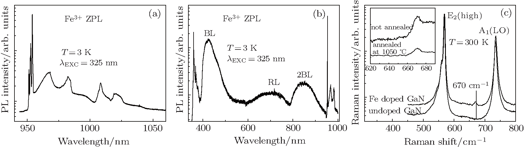 | Fig. 4. (a) A series of characteristic IR luminescence with a sharp zero-phonon line (ZPL) at 1.299 eV at low temperature, (b) quenching of the intensity of near band edge excitonic emissions in the UV region, (c) a kind of phonon mode originating from VN. |
Compensation mechanisms of GaN:Fe have attracted much more attention, since these are important to the optical, electrical, and magnetic properties of the crystal.[64, 74] The Fe atoms incorporated in GaN matrix substitute in Ga sites and introduce the charge transfer level 
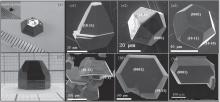
In 1997, Yamane et al.[15] reported that GaN crystal can be grown in a Ga– Na mixed solution in relatively low pressure nitrogen atmosphere (< 50 atm) and at a relatively low temperature range of 600 ° C– 900 ° C called the Na-flux method. The Na-flux method has a significant advantages in synthesizing high quality GaN crystal through spontaneous nucleation process with very simple equipment. Imade et al.[78– 80] reported that the GaN bulk crystal could be grown on the small spontaneously nucleated GaN seed by a long growth period, as shown in Figs. 5(a) and 5(b). In our group, we also obtain the GaN single crystals by spontaneous method, with the help of high-temperature and high-pressure home-made autoclave. Figures 5 [(a1)– (a3) and (b1)– (b3)] show the morphology of the spontaneously nucleated GaN crystals grown by Na flux. However, it is difficult to grow large GaN crystals with a moderate growth rate, because of the difficulty in controlling the spontaneous nucleation process.
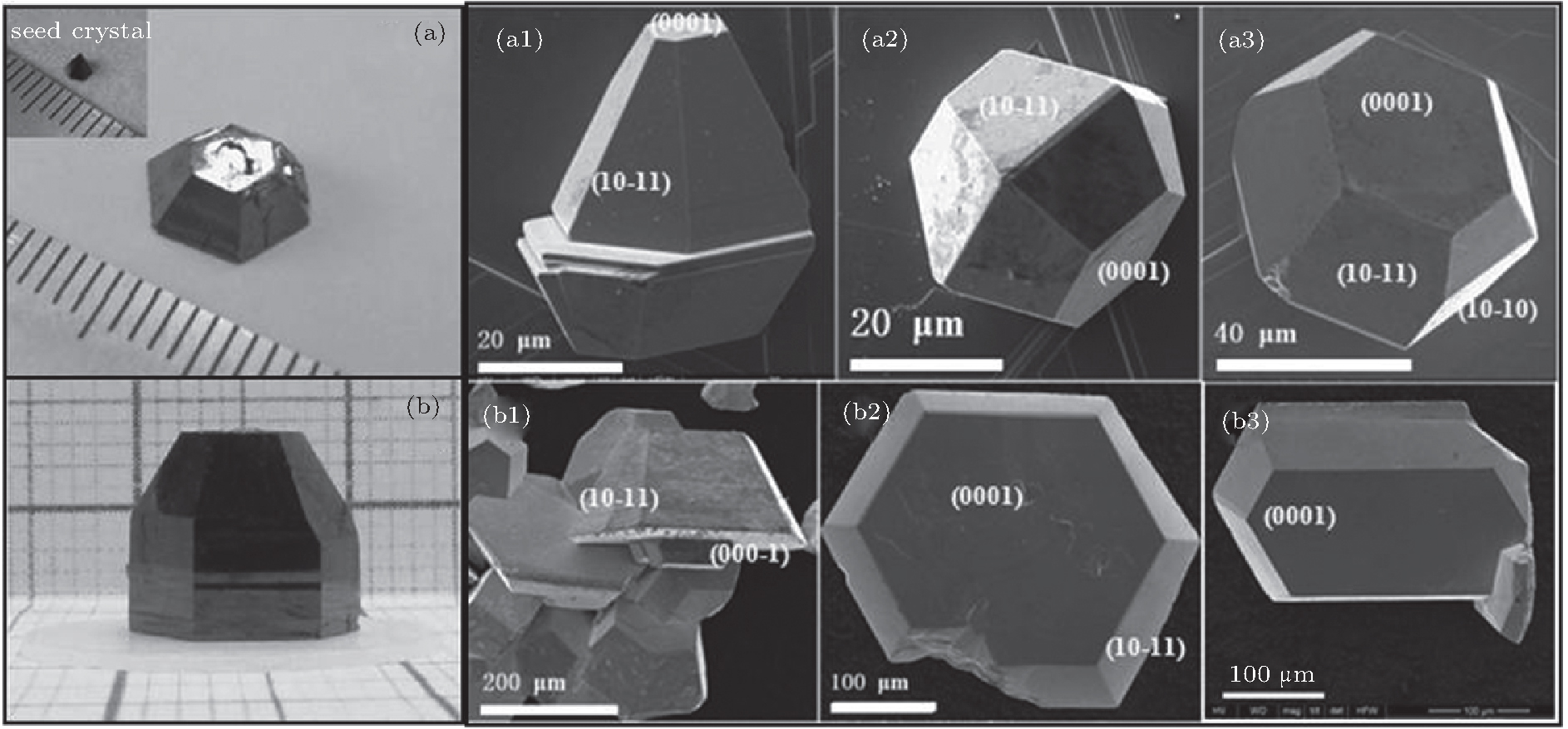 | Fig. 5. (a) and (b) Photographs of GaN bulk crystal grown on the small spontaneously nucleated GaN seed by a long growth period. (from Refs. [78] and [79]); (a1)– (a3) and (b1)– (b3): Morphology of the spontaneously nucleated GaN crystals grown by Na-flux method. (Temperature: 973 K∼ 1073 K, pressure: 2.0 MPa∼ 3.5 MPa). |
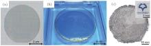
In 2003, a group at Osaka University employed the liquid phase epitaxy (LPE) method using Na flux and made major progress in terms of the GaN single crystal size and quality, as well as scalability of the crystal growth system.[81– 83] In 2008, a 3-mm thick 2-inch GaN crystal was obtained for the first time by adding carbon additive in the Na-flux method.[84] In recent years, Osaka University has succeed in growth of 4-inch GaN bulk crystal[80] and high quality GaN bulk crystal with dislocation densities less than 103/cm2[85] (Fig. 6). These important results were encouraged by the collaboration between Osaka University and Nichia/Ricoh Co., Ltd.
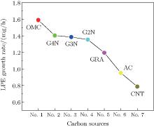
Aiming to improve the yield of the liquid phase epitaxy GaN, Kawamura et al.[84] found that the addition of carbon could effectively suppress the generation of polycrystals, which could also improve the growth rate. Mori et al.[19] investigated the dependence of growth rate on the concentration of carbon, and reported that an increase of carbon in the solution enhanced the growth of GaN at low concentrations and tended to suppress the GaN growth at higher concentrations. In our study, we found that the type of carbon used has an effect on the generation and morphology of GaN polycrystals, while the growth rate of the liquid phase epitaxy single crystals decreased in the following order: OMC, G4N, G3N, G2N, GRA, AC, and CNT, [86] as shown in Fig. 7. Though only 18 years have passed since the Na-flux method was discovered, significant results have been reported. The Na-flux method has a great potential to realize the GaN bulk single crystal and industrialized production.
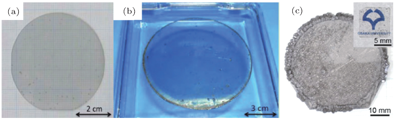 | Fig. 6. (a) 2-inch and (b) 4-inch GaN crystals grown on HVPE-GaN seed crystals by Na-flux method (from Ref. [80]), (c) morphology of 2-inch coalesced GaN crystal (from Ref. [85]). |
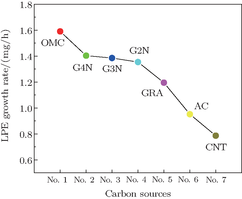 | Fig. 7. The LPE growth rate of GaN single crystal grown on HVPE substrate with different carbon sources (from Ref. [86]). |
The foundation of the ammonothermal method is built upon the discovery that GaN dissolves into supercritical ammonia under certain conditions. Currently, it is possible to dissolve up to ∼ 1 at.% of GaN into a supercritical ammonia solution with additives, also called mineralizers. The mineralizers, commonly used at present, can be divided into two typical kinds: ammono bases (amides, such as LiNH2, NaNH2, and KNH2), and ammono acids (alkali halides, such as NH4Cl, NH4Br, and NH4I). The addition of alkali metals will result in a basic alkaline ammonia solution, whereas the addition of halogens will result in an acidic ammonia solution. It is possible to grow GaN using either solution, with each exhibiting its own unique traits.
The first ammonothermal synthesis demonstration for III-nitrides was performed in 1982. It was initiated in 1990s, when Dwilinski et al. showed that it was possible to obtain a fine-crystalline GaN by a chemical reaction between gallium and ammonia, in the presence of alkali-metal amides (LiNH2 or KNH2), realizing the potential of the method as a prospective candidate for bulk GaN crystal growth.[87] Since 2000, many groups got involved in ammonothermal growth, in both ammonobasic and ammonoacidic environments. It was not until the 2010s that the method evolved strongly through the point of the availability of boules that are greater than two inches in diameter and exceed 10 mm in height with exceptional crystal quality.[27] The typical temperatures and pressures applied are 0.1 GPa– 0.3 GPa and 500 ° C– 600 ° C, respectively. The growth rates to 10 μ m/h were achieved in order to keep high quality seeds.
Furthermore, the crystal quality of the GaN crystals grown using the basic ammonothermal method have threading dislocations below 104 cm− 2 and c-plane lattice curvatures are on the order of a hundred meters, as compared to ∼ 10 m for HVPE material. The crystal quality as measured by the FWHM of the omega rocking curve is lower than 20 arcsec, suggesting a perfect crystal.[88] In addition, the ammonothermal method has thus far been the only method to demonstrate truly large non-polar and semi-polar substrates based on the slicing of a bulk single-crystal GaN boule.[89] From photoluminescence spectra measured at 10 K, both free excitons and biexciton transitions were observed, which is an indicator of a high-quality sample. In addition, it appears that the density of SFs in m-plane GaN is negligible, given the absence of an emission band at 3.42 eV, which is the signature of SFs.[90] The carrier concentration of the wafers can be controlled by appropriate doping. N-type, p-type, and semi-insulating substrates can be grown via the ammonothermal method, as measured by both Hall effect experiments and contactless methods. High quality of homoepitaxial layers deposited on AMMONO-GaN substrates was also confirmed by optical measurements.[91, 92]
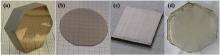
Acidic mineralizers have also been employed to synthesize free-standing hexagonal GaN crystal and homoepitaxial films. In 2008, Ehrentraut et al. reported the first attempt on the acidic ammonothermal growth of GaN on a 2-inch HVPE seed crystal.[93] About 0.5-mm thick ammonothermal GaN has been grown. However, the crystal quality is unsatisfying at this stage of research, the FWHM of x-ray rocking curve value is not lower than 52 arcsec– 63 arcsec, with dislocation density 106 cm− 2, due to using the HVPE seeds. More recently, Soraa has developed a novel ammonothermal approach, utilizing internal heating to circumvent the material property limitations of conventional ammonothermal reactors, to grow (0001) GaN with diameters up to two inches (Fig. 8(d)).[94, 95] High crystallinity GaN with FWHM values about 20 arcsec– 50 arcsec dislocation densities below 1 × 105 cm− 2 have been obtained. High optical transmission was achieved with an optical absorption coefficient below 1 cm− 1 at a wavelength of 450 nm.
 | Fig. 8. (a) Photograph of a thick 1-inch a-GaN bulk crystal (from Ref. [90]), (b) photograph of 2-inch c-plane A-GaN substrate (from Ref. [27]), (c) photograph of 1-inch m-plane A-GaN crystal (manufactured at AMMONO company) (from Ref. [27]), (d) photograph of a 2-inch (0001) SCoRA GaN crystal grown on an SCoRA seed (from Ref. [94]). |
While the ammonothermal method has already shown great promise, there are many challenges that still need to be overcome to achieve true commercialization. The four most important challenges are improved growth rates, reduced impurity levels, improved transparency, and availability of large seeds in sufficient quantity for mass production.[96– 104] Focusing on the key issues to be resolved, many groups gradually carry out the research in both ammonobasic and ammonoacidic environments.
Generation of large area, high quality seed crystals in large quantities using the ammonothermal method is challenging and time consuming due to slow growth rates, particularly in the m-plane direction. The results of growth rates in different crystallographic directions and morphology investigations were published.[105– 107] It was reported that the total growth rates can be improved to (344± 30) μ m/day for c-plane growth and (46± 2) μ m/day for m-plane growth.[97]
It is challenging to remove the impurities from the growth environment, due to the corrosive nature of the supercritical ammonia solution and the lack of ultra-high purity materials used for growth. Generally, the introduction of an Ag or Pt capsule into the autoclave will yield a high purity growth environment, and then transition metal impurities in the GaN crystals were reduced to less than 1 × 1017 cm− 3 and oxygen impurity concentrations were comparable to those of the polycrystalline HVPE GaN source material (1 × 1019 cm− 3).
The GaN substrates in Fig. 8 are colored because of the incorporation of oxygen and/or transition metal impurities from polycrystalline HVPE GaN source material and autoclaves. If ammonothermal GaN substrates are to be used for LEDs, it is critical to improve the optical absorption losses. For lasers and electronic devices, the optical transparency is not as critical. It is desired to have absorption coefficients below 1 cm− 1 for the wavelengths of interest. A typical ammonothermal GaN using the current technique yields a brownish or yellowish tinted crystal. The approximate optical coefficient is around 5 cm− 1 for these films. Lower values are needed and most likely will result from a reduction in impurity concentration. It is still an open question whether some coloration results from the formation of intrinsic point defects, such as Ga or N vacancies, impurities, off– stoichiometry, or other crystal imperfections.
A full understanding of dislocation nucleation, multiplication, and movement behavior is essential to decrease the dislocation density in GaN substrate and develop advanced technologies for improving GaN-based device performance.
Nanoindentation is an ideal method for studying the dislocation behavior in a crystal.[108] There has been a considerable effort to determine the properties of dislocation in GaN during plastic deformation using indentation.[109, 110] However, most of these earlier studies mainly focused on the microstructure of the plastic deformation in GaN thin film, so the fundamental dislocation multiplication and movement mechanism of GaN substrate are not understood fully.
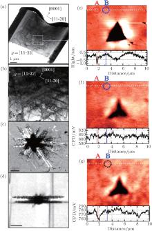
A combination of nanoindentation and CL techniques has been performed to investigate the movement mechanism of dislocations in a GaN substrate under nanoindentation by Huang and Xu et al.[111] The experimental results show that the plastic deformation of c-plane GaN is primarily due to slip occurring on both {001} and {101-1} planes. Dislocation loops can multiply and move from plane to plane by cross-slip after nucleation, enabling the plastic deformation to proceed further. This mechanism is further supported by the remarkable movement of the indentation-induced dislocations during annealing (Figs. 9(a)– 9(d)).
 | Fig. 9. (a) and (b) Dark-field XTEM images of indentation in c-plane GaN; Room-temperature panchromatic CL images of conical indent in GaN (c) Dislocation luminescence in c-plane GaN under nanoindentation; (d) Dislocation pattern in m-plane GaN under nanoindentation; (e) The topographic image around a nanoindentation with a scan area of 10 μ m × 10 μ m. A V-pit of thread dislocation is marked with A, and a nearby plane position is marked with B. Panels (f) and (g) are the CPD images of the same area acquired under dark conditions and under UV illumination with wavelength of 360 nm, respectively. The curves in the images are profiles along the white line.[114] |
Further Huang and Xu et al. also demonstrated the nanoscale anisotropic dislocation behavior in GaN subs-trate.[112] They presented nanoindentation experiments performed on the three principal surfaces, (0001), (11-20), and (10-10), of GaN substrate. CL and cross-sectional transmission electron microscopy (XTEM) measurements show that there are two primary dislocation slip planes ((0001) and (10-11) planes) for c-plane GaN, while there is only one most favorable dislocation slip plane ((0001) plane) for nonplanar GaN during plastic deformation. They suggest that the anisotropic elasto-plastic mechanical properties of GaN are relative to its anisotropic plastic deformation behavior.
More interesting, of course, are the intrinsic optical properties of dislocations in GaN substrate. A VL band peaking at about 3.12 eV from the region near the dislocations is characterized and identified by Huang and Xu et al.[113] A comprehensive study encompassing CL, Raman, and annealing experiments allowed the assignment of VL band to e– A transitions involving VGa. They proposed the VGa is formed by the motion of jogged dislocations under shear stress.
The dislocations strongly affect the carrier properties in GaN, including minority diffusion lengths and surface recombination velocities, both of which are important for device performance. For example, in photovoltaic detectors, due to a large absorption coefficient of GaN, carriers are generated close to the surface and recombine. A sufficiently long minority diffusion length and the suppression of surface recombination velocity are helpful in the realization of high sensitivity.[115] However, for most characterization methods, such as photoluminescence, [116] surface photovoltage, [117] and photocurrent[118] measurements, the spatial resolution of as-measured carrier properties is low, which makes it difficult to reveal the relationship between the experimental results and the local dislocation structures. Electron beam-induced current (EBIC) method is capable of achieving the inhomogeneity of minority diffusion length along a depth gradient, but a p– n junction or a Schottky barrier has to be made at a cross section.[119] Recently, a combination of surface photovoltage spectroscopy (SPS) method and Kelvin probe force microscopy (KPFM) was reported for simultaneous measurement of the topography, the local minority diffusion length and the surface recombination velocity at a single thread dislocation.[114] The contact potential difference (CPD) at nanometer scale, varying with the incident photon energy, was measured with a corresponding topography image. SPS responses at single thread dislocations near a nanoindentation on an HVPE-grown GaN surface can be distinguished. As shown in Figs. 9(e)– 9(g), the thread dislocations introduced by a nano-indentation were observed as V-pits, where the photovoltage was lower than that on the plane surface under ultra-violate illumination. Compared with those on the plane surface, the calculated hole diffusion length is 90 nm shorter and the surface electron recombination velocity is 1.6 times higher at an individual thread dislocation.
The usefulness of bulk GaN substrates in device fabrication was confirmed (LEDs, LDs, and power devices), boosting much hope for applications of the bulk GaN production of high optical-power light emitters and other microelectronic devices.
GaN substrates can offer three different benefits for fabrication of InGaN-based laser diodes (LDs). First, smooth facets can be obtained by cleaving along the m-plane by using GaN substrates, which helps reduce the threshold current density and improve fabrication yield. Second, vertical LD structure can be fabricated by depositing n-electrode on the N-face of GaN substrates, which eliminates the current crowding effect that exists in lateral LD structures, and thus reduces operation voltage. Third, the lifetime of InGaN-based LDs can be improved by using GaN substrates with low dislocation density since dislocation defects can seriously reduce the lifetime of InGaN-based LDs operated at current density of more than 5 kA/cm2
By employing high quality GaN substrates, the performance of GaN-based laser diodes has made great advances in the past several years. Blue laser diodes with threshold current density lower than 2 kA/cm2 and output power higher than 1 W have been commercialized by Nichia[120] and Osram.[121] However, epitaxial growth on bulk GaN substrates is not straightforward and the details about home-epitaxy have rarely been reported. At Suzhou Institute of Nano-tech and Nano-bionics, we have carried out extensive studies on the homo-epitaxy of GaN-based laser diodes on bulk GaN substrates. We have found that one key factor that affects the quality of epilayer grown on bulk GaN substrates is the miscut angle. A miscut angle larger than 0.2° is needed to suppress hillocks and wavy morphology.[122] We have also obtained blue LDs with low threshold current, low voltage, and high output power. Power– current– voltage curves of a blue InGaN LD packaged with TO-56 under room-temperature (RT) and continuous-wave (CW) conditions are shown in Fig. 10(a). At the current of 650 mA, light output power is 500 mW and voltage is 5.8 V, which means a wall-plug efficiency of 13%.
In contrast, it took more than a decade to realize GaN-based green laser diodes due to several challenges, which include incompatibility of growth conditions of In-rich InGaN quantum wells (and GaN and AlGaN as well), large lattice mismatch between In-rich InGaN quantum wells and GaN, and reduced optical confinement due to smaller difference of refractive index between InGaN and AlGaN. The former two issues result in a high density of defects[123– 126] and broadened gain spectra.[127– 130] After great efforts to develop green laser diodes by many groups during the past decade, lasing in the green spectrum range has been realized by several groups such as Nichia, [131] Sony and Sumitomo, [132, 133] Osram, [134, 135] UCSB, [136, 137] Corning, [138] and Soraa.[139, 140] We have also been developing green laser diodes on c-plane bulk GaN substrates. Green LD structures with excellent luminescence homogeneity and small linewidth have been fabricated on Nanowin’ s ultra-high quality GaN substrates.[141, 142] Lasing has been achieved, [142] as shown in Fig. 10(b). The threshold current at room temperature is 400 mA under pulse operation with 300-ns pulse width and 10-kHz repetition frequency.
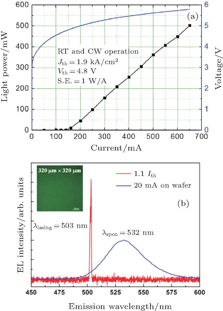 | Fig. 10. (a) Power– current– voltage curves of a blue InGaN LD packaged with TO-56 under room-temperature and continuous-wave conditions; (b) EL spectra of green LD below and above threshold current. Inset shows micro-PL image of the green LD structure, indicating homogeneous luminescence and no dark spot. |
The LED market grew rapidly in recent years, reaching 50 million US dollars last year. However, most LEDs in the market are based on foreign substrates because the volume production GaN bulk substrates are still under improvement, and the cost is relatively high. The main challenge inherent in today’ s LEDs is the efficiency droop effect; the related influencing aspects are still under discussion.[143] Growing LEDs by homo-epitaxy based on GaN bulk is a possible route. Cao et al. were first to demonstrate UV and blue LEDs grown on GaN bulk substrate. The internal quantum efficiency of the UV LED on GaN was higher compared to the UV LED on sapphire, whereas the performance of the blue LEDs was found to be comparable.[144] Since then, more and more research groups and companies are interested in research on LEDs on GaN bulk substrates.[145, 146] The performance of LEDs grown on GaN bulk substrate has achieved quite remarkable progress in recent years. In 2012, Soraa reported an external quantum efficiency of 68% at 180 A· cm− 2 and no current crowding is observed at high current density.[147] Then Soraa upgrade the extraction efficiency to 89%[148] in 2014, and total power conversion efficiency to 84%[149] in 2015. Besides the above-mentioned LEDs grown on the Ga-face GaN, LEDs grown on non-polar GaN substrates are another hot research field because of the reduction of quantum-confined Stark effect in this structure. Sato et al. demonstrated a green LED with a peak emission wavelength of 516 nm grown on semipolar (11-22) bulk GaN substrate in 2007.[150] The performance has improved significantly in recent years.[151] However, suffering from the size limitation of non-polar GaN bulk substrates, the market application of non-polar LEDs is quite confined.
Power semiconductor devices are the key building block for power electronic systems like solar inverters, electric vehicle drives, the three-phase motor driver in hybrid vehicles, and so on. With the wide band gap and thus high critical field, GaN is a promising material for high power devices and has attracted much attention since silicon power devices are approaching physical limits of the materials. While high power devices based on SiC are more mature, GaN-based devices have the potential to be better because the fundamental (material based) figure of merit (FOM) parameters for GaN are larger than those of SiC.[152] However, the performance and reliability of most lateral GaN-based power devices have fallen short of their potential because the quality of GaN layers grown on foreign substrates (e.g. sapphire or Si) is poor due to the high dislocation density (> 108 cm− 2) and because lateral device architectures are less well suited for high voltage and high current power applications. Low defect density is important for power devices because it can affect the performance characteristics (e.g. breakdown voltage and off-state leakage current), yield, and reliability. By fabricating the power devices on high-quality bulk GaN substrates, realizing the material limit potential of GaN is expected to be possible including true avalanche breakdown capability, to create vertical architectures that do not suffer from the thermal management issues, and to permit an increased number of die on a wafer and improve device reliability. Recently, a variety of GaN-based power devices have been successfully obtained on the bulk GaN substrates. For example, Nie et al.[153] fabricated vertical GaN transistors using 2-inch bulk GaN substrates with a low dislocation density (104 cm− 2), and the transistors exhibit saturation current exceeding 2.3 A, breakdown voltages of 1.5 kV, area differential specific on-resistance of 2.2 mΩ · cm2, and an FOM of 1.0 × 10⁹ V2 · Ω − 1· cm− 2 with a junction termination extension scheme. Freestanding GaN substrates were also used to fabricate submicrometer gate-length (LG) high electron mobility transistors (HEMTs) with excellent dc and RF performance, [154] and LG = 100 nm devices exhibited a drain current density of 1.5 A/mm, current gain cutoff frequency fT of 165 GHz, a maximum frequency of oscillation fmax of 171 GHz, and intrinsic average electron velocity of 1.5 × 107 cm/s. The vertical breakdown voltage of the heterostructure field effect transistor (HFET) on the Na-flux grown GaN substrate is reported to be over 3000 V for a GaN buffer layer thickness of 10 μ m, giving a breakdown field of 3.2 MV/cm, almost equal to the physical limit of GaN (3.3 MV/cm).[78] Besides that, vertical p– n diodes are also successfully fabricated on pseudo-bulk low defect density (104 cm− 2– 106 cm− 2) GaN substrates, [155] and the measured devices demonstrate near power device figure of merit, that is, differential specific on-resistance of 2 mΩ · cm2 for a breakdown voltage of 2.6 kV and 2.95 mΩ · cm2 for a 3.7 kV device, respectively. In 2010, Saitoh et al.[156] fabricated the vertical GaN Schottky barrier diodes (SBDs) with field plate structure on freestanding GaN substrates, and the specific on-resistance (RonA) and the breakdown voltage (VB) of the SBDs were 0.71 mΩ · cm2 and over 1100 V, respectively. The figure of merit 
Nitride materials are suitable for high-efficiency tandem solar cells.[158, 159] The band gaps of InGaN ternary alloys have a broad range from 0.65 eV to 3.43 eV, which offers a high degree of freedom in the design of tandem solar cells. And a maximum conversion efficiency of close to 65% is expected by utilizing multiphoton absorption.[160] However, in practice it is difficult to fabricate high-efficiency photovoltaic cells from InGaN. First of all, indium incorporation and segregation easily occur because of the large lattice mismatch between InN and GaN.[161] Secondly InxGa1− xN films suffer from lattice mismatch with the most common substrates such as sapphire and silicon.[162] To overcome these challenges and improve the crystal quality in the high-effeciency InGaN photovoltaic (PV) devices, it is currently considered that growing InGaN films on the freestanding GaN substrate is an important approach.[163] The conversion efficiency of the InGaN-based solar cell on the GaN substrate reached 1.4%, approximately 1.5 times that of solar cells on sapphire substrate.[164]
An investigation of correlations between PV performance and crystal defects demonstrated that the reduction of pit density using high-quality GaN substrate is essential for the realization of high-performance InGaN-based solar cells.[165] Using a low-TDD GaN substrate prevented the generation of V-shaped defects and increased open-circuit voltage from 1.6 V to 2.2 V and conversion efficiency by 40%.[166] By the growth of the high-quality InGaN/InGaN superlattice active layer on a GaN substrate, Kuwahara et al. obtained a high conversion efficiency of 2.5% for the InGN-based solar cell.[164] Young et al. also confirmed that GaN substrate outperformed sapphire substrate in their investigation of high performance InGaN/GaN MQW solar cells.[167] Most recently, Young et al. further obtained a conversion efficiency of 3.33% under the AM0 spectrum for InGaN solar cell fabricated on the GaN substrates by integrating well-designed broadband optical coatings.[168]
In summary, the performance of InGaN-based solar cell on GaN substrate is still in progress, and it is necessary to improve the quality of GaN substrate further for the fulfillment of higher-efficient InGaN-based solar cells. Especially GaN substrates with TDD lower than 103 cm− 2 ∼ 104 cm− 2, no V-shaped defects, and high doping will be the key for developing PV devices.
Different growth methods of bulk GaN have been developed in recent years, with rapid progress mainly in two dimensions: step-by-step enlargement of wafer size and gradual reduction of dislocation density. So far, the biggest bulk GaN wafer is about 6 inches in diameter, and the GaN substrate diameter for volume production is mainly about two inches, primarily manufactured by HVPE. The typical dislocation density of GaN grown by HVPE is about 106 cm− 2, which can be reduced to 104 cm− 2 by overgrowth on GaN nanorods. Employing sodium-flux and ammonothermal growth, the dislocation density of GaN substrate is now about 103 cm− 2 and 104 cm− 2, with the largest wafer diameter about two inches and four inches, respectively. The lowest dislocation density is obtained by high-pressure high-temperature growth, with a limit size of about several millimeters. Regardless of any of the above-mentioned growth methods, the growth rate of Ga-plane or N-plane is fairly higher than the other nonpolar or semi-polar planes; the size of nonpolar and semi-polar GaN substrates is still very limited, not really meeting the existing application demand.
Doping of bulk GaN substrate is another important issue for device application. Un-doped n-type, Si-doped n-type, and Fe-doped semi-insulating type GaN substrates are well developed and successfully applied in different devices, such as LEDs, LDs, power devices, and so on. On the other hand, research on P-type doping and intrinsic semi-insulating bulk GaN substrate is still in the initial stage.
Looking to the future, bulk GaN substrates will play more and more important roles in the application of III-nitride-based semiconductor devices, by homo-epitaxy and device structure innovation substituting for hetero-epitaxy and the device structure now in use. The volume of bulk GaN substrate will grow rapidly for several years to come, with bigger size, higher quality, and lower cost. To realize the mass production and wide application of bulk GaN substrates, the combination of different growth methods is a possible solution. On the other hand, the development of larger size nonpolar and semi-polar bulk GaN substrates, the realization of p-type and intrinsic semi-insulating bulk GaN substrate will enable new applications.
Thanks a lot for the GaN team members, Mr. Cai De-Min, Mr. Xu Yu, Mrs. Wang Ming-Yue, Zhang Yu-Min, and Hu Xiao-Jian, for their efforts in HVPE growth and characterization. Thanks to Dr. Liu Jian-Ping, Dr. Huang Jun, and Dr. Liu Zong-Liang, for their contributions in experiments work and help in preparing the manuscript.
| 1 |
|
| 2 |
|
| 3 |
|
| 4 |
|
| 5 |
|
| 6 |
|
| 7 |
|
| 8 |
|
| 9 |
|
| 10 |
|
| 11 |
|
| 12 |
|
| 13 |
|
| 14 |
|
| 15 |
|
| 16 |
|
| 17 |
|
| 18 |
|
| 19 |
|
| 20 |
|
| 21 |
|
| 22 |
|
| 23 |
|
| 24 |
|
| 25 |
|
| 26 |
|
| 27 |
|
| 28 |
|
| 29 |
|
| 30 |
|
| 31 |
|
| 32 |
|
| 33 |
|
| 34 |
|
| 35 |
|
| 36 |
|
| 37 |
|
| 38 |
|
| 39 |
|
| 40 |
|
| 41 |
|
| 42 |
|
| 43 |
|
| 44 |
|
| 45 |
|
| 46 |
|
| 47 |
|
| 48 |
|
| 49 |
|
| 50 |
|
| 51 |
|
| 52 |
|
| 53 |
|
| 54 |
|
| 55 |
|
| 56 |
|
| 57 |
|
| 58 |
|
| 59 |
|
| 60 |
|
| 61 |
|
| 62 |
|
| 63 |
|
| 64 |
|
| 65 |
|
| 66 |
|
| 67 |
|
| 68 |
|
| 69 |
|
| 70 |
|
| 71 |
|
| 72 |
|
| 73 |
|
| 74 |
|
| 75 |
|
| 76 |
|
| 77 |
|
| 78 |
|
| 79 |
|
| 80 |
|
| 81 |
|
| 82 |
|
| 83 |
|
| 84 |
|
| 85 |
|
| 86 |
|
| 87 |
|
| 88 |
|
| 89 |
|
| 90 |
|
| 91 |
|
| 92 |
|
| 93 |
|
| 94 |
|
| 95 |
|
| 96 |
|
| 97 |
|
| 98 |
|
| 99 |
|
| 100 |
|
| 101 |
|
| 102 |
|
| 103 |
|
| 104 |
|
| 105 |
|
| 106 |
|
| 107 |
|
| 108 |
|
| 109 |
|
| 110 |
|
| 111 |
|
| 112 |
|
| 113 |
|
| 114 |
|
| 115 |
|
| 116 |
|
| 117 |
|
| 118 |
|
| 119 |
|
| 120 |
|
| 121 |
|
| 122 |
|
| 123 |
|
| 124 |
|
| 125 |
|
| 126 |
|
| 127 |
|
| 128 |
|
| 129 |
|
| 130 |
|
| 131 |
|
| 132 |
|
| 133 |
|
| 134 |
|
| 135 |
|
| 136 |
|
| 137 |
|
| 138 |
|
| 139 |
|
| 140 |
|
| 141 |
|
| 142 |
|
| 143 |
|
| 144 |
|
| 145 |
|
| 146 |
|
| 147 |
|
| 148 |
|
| 149 |
|
| 150 |
|
| 151 |
|
| 152 |
|
| 153 |
|
| 154 |
|
| 155 |
|
| 156 |
|
| 157 |
|
| 158 |
|
| 159 |
|
| 160 |
|
| 161 |
|
| 162 |
|
| 163 |
|
| 164 |
|
| 165 |
|
| 166 |
|
| 167 |
|
| 168 |
|