Progress in bulk GaN growth
Xu Kea), b)†  , Wang Jian-Feng
a), b) , Ren Guo-Qianga), b)
, Wang Jian-Feng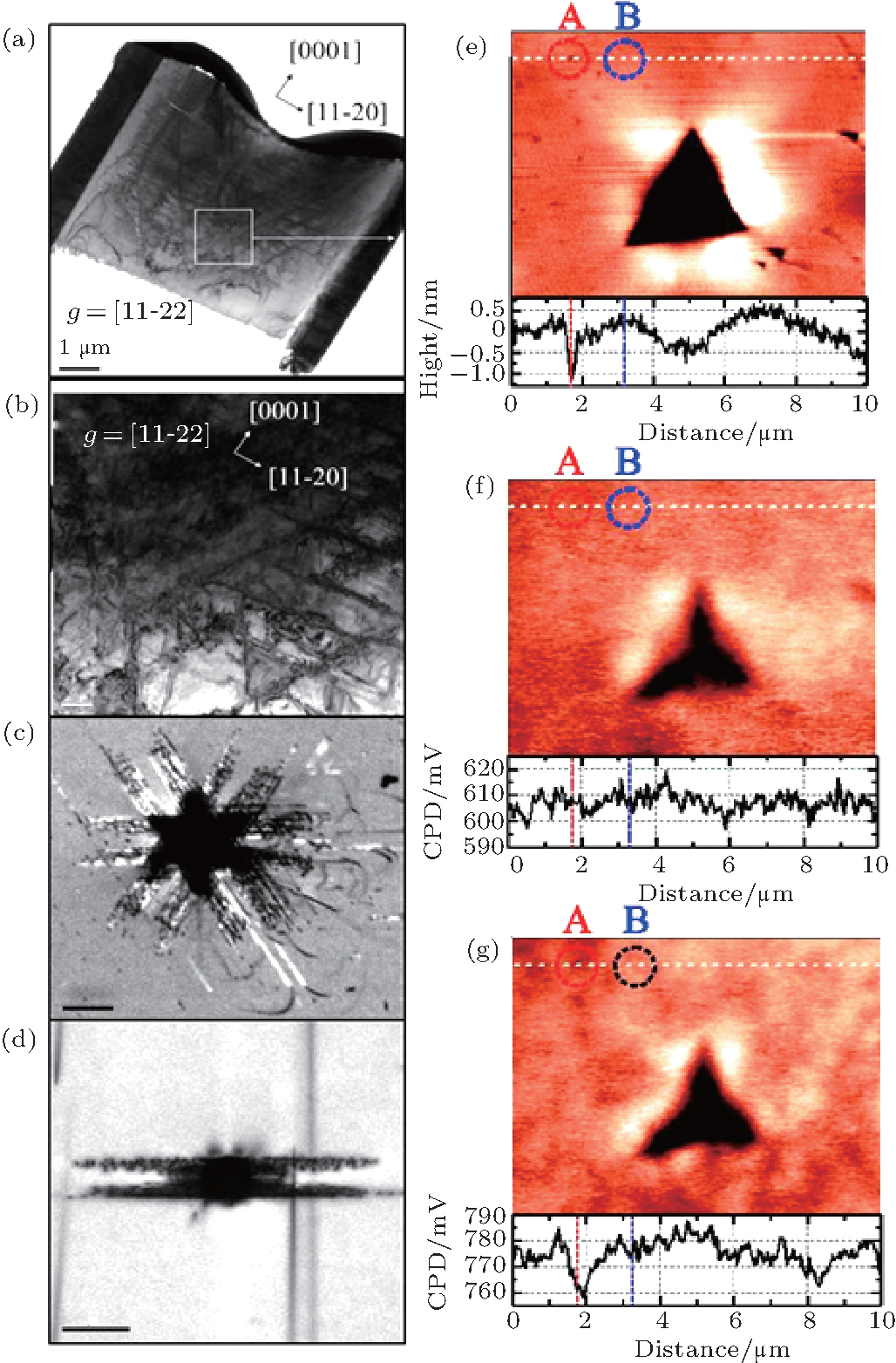
Progress in bulk GaN growth |
|
Xu Ke
, Wang Jian-Feng |
| (a) and (b) Dark-field XTEM images of indentation in c -plane GaN; Room-temperature panchromatic CL images of conical indent in GaN (c) Dislocation luminescence in c -plane GaN under nanoindentation; (d) Dislocation pattern in m -plane GaN under nanoindentation; (e) The topographic image around a nanoindentation with a scan area of 10 μm × 10 μm. A V-pit of thread dislocation is marked with A, and a nearby plane position is marked with B. Panels (f) and (g) are the CPD images of the same area acquired under dark conditions and under UV illumination with wavelength of 360 nm, respectively. The curves in the images are profiles along the white line.[ 114 ] |
| |