Liu Jian-Ming, Zhang Jie, Lin Wen-Yu, Ye Meng-Xin, Feng Xiang-Xu, Zhang Dong-Yan, Steve Ding, Xu Chen-Ke, Liu Bao-Lin. Effect of pressure on the semipolar GaN (10-11) growth mode on patterned Si substrates* . Chinese Physics B, 2015, 24(5): 057801
Permissions
Effect of pressure on the semipolar GaN (10-11) growth mode on patterned Si substrates*
Liu Jian-Minga)†, Zhang Jiea), Lin Wen-Yua), Ye Meng-Xina), Feng Xiang-Xua), Zhang Dong-Yana), Steve Dinga), Xu Chen-Kea), Liu Bao-Linb)
Sanan Optoelectronics Techonology LTD, Xiamen 361009, China
Department of Physics, Xiamen University, Xiamen 361005, China
Project support by the National High Technology Research and Development Program of China (Green Laser).
Abstract
In this paper, we investigate the effect of pressure on the growth mode of high quality (10-11) GaN using an epitaxial lateral over growth (ELO) technique by metal organic chemical vapor deposition (MOCVD). Two pressure growth conditions, high pressure (HP) 1013 mbar and low pressure growth (LP) 500 mbar, are employed during growth. In the high pressure growth conditions, the crystal quality is improved by decreasing the dislocation and stack fault density in the strip connection locations. The room temperature photoluminescence measurement also shows that the light emission intensity increases three times using the HP growth condition compared with that using the LP growth conditions. In the low temperature (77 K) photoluminescence, the defects-related peaks are very obvious in the low pressure growth samples. This result also indicates that the crystal quality is improved using the high pressure growth conditions.
Keyword:
78.55.-m; 78.30.Fs; semipolar; pressure; metal-organic chemical vapor deposition
Although GaN has been widely used in electronic and optical devices, [1– 3] the conventional c-plane optical devices still suffer from the quantum-confined Stark effect (QCSE) due to the spontaneous and piezoelectric polarization fields parallel to the [0001] direction.[2, 4] This effect restricts the carrier recombination efficiency, reduces the oscillator strength, and induces a red-shift in photon emission. Compared with the c-plane light-emitting diodes (LEDs), the semi-polar LEDs exhibit a smaller blue shift of the peak and a lower efficiency droop at high injection current and it is easier to obtain long wavelength emission.[4, 5]
Because it is very expensive to use free standing GaN as a substrate, most of the GaN-based epitaxial growth is performed on sapphire, SiC, or Si substrates. Si substrates have been considered as one of the good choices due to its low manufacturing cost, large size, and good thermal and electrical conductivities.[6] However, there are still several problems in the growth of GaN on the Si substrates. First, the lattice mismatch between GaN and Si is about 17%, leading to high threading dislocation density (∼ 109– 1011 cm-2) in the GaN epilayer. Second, because the thermal expansion coefficient difference between Si and GaN is 56%, a lot of cracks and damages are generated in the GaN epilayer during cooling in the growth process.[7] One of the approaches to solve these problems is to use patterned Si substrates for selective area growth (SAG) and epitaxial lateral over growth (ELO).[8, 9] High quality semi-polar GaN has been obtained by epitaxial growth on patterned Si substrates.[10, 11] Despite the previous studies, [9, 10] the effect of pressure on the (10-11) GaN quality and growth mode base on the patterned Si substrates has not been reported yet. In this paper, we investigate the evolution of growth mode of the (10-11) semi-polar GaN under different pressure growth conditions.
2. Experiment procedure
The (10-11) GaN was grown on an 8° off-oriented n-type (001) Si substrate by selective region growth using a metal-organic chemical vapor deposition (MOCVD) system. Conventional precursors, including trimethylgallium (TMGa), trimethylaluminum (TMAl), and ammonia, were used to grow GaN. Hydrogen was used as a carrier gas for growth of GaN. The patterned substrate was prepared as follows. First, we prepared a (001) Si substrate, its 〈 001〉 axis tilts 8° toward the 〈 110〉 direction. The stripe pattern in the Si substrate was fabricated with optical lithography, followed with wet etching in a 25% KOH solution for 2.5 min at 42 ° C. The strip pattern has a period of 1 μ m (groove)/1 μ m (stripe). The depth of the grooves is 0.6 μ m. The (-1-11) facet of the groove sidewalls was passive by SiO2 deposition and the (111) facet was exposed to air for GaN growth. The AlN buffer layer was deposited at 1250 ° C for 20 min (determined by a thermocouple), and the thickness was about 100 nm, as estimated from scanning electron microscope (SEM) measurements. The GaN was selectively grown on the (111) facet following the AlN buffer layer. The first GaN layer was deposited at 1200 ° C and with a V/III ration of 2288 for 15 min. Two groups of conditions were used for the growth of the first GaN layer: one at pressure of 500 mbar (LP) and the other at 1013 mbar (HP). The growth conditions are summarized in Table 1.
Table 1.
Table 1.
Table 1. Growth conditions of semipolar GaN.
Pressure/mbar
Symbol
Growth condition
1013
A
1190 V/III 305
B
1150 V/III 305
500
C
1190 V/III 305
D
1150 V/III 305
Table 1. Growth conditions of semipolar GaN.
The surface morphology was investigated via SEM. The dislocation, stack fault distribution, and growth mode were determined by cathodoluminescence (CL) spectra with a 10 kV accelerating voltage at room temperature. Both the CL and the SEM were obtained by using a JEOL 4300 system and a Gantan detector. An optical grating of 1200/μ m was used for the CL spectra. The photoluminescence (PL) measurement with the 325 nm laser was also conducted at room temperature and low temperature (77 K) respectively.
3. Results and discussion
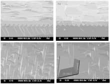
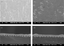
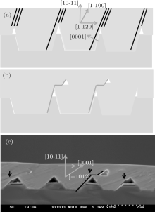
The growth temperature and pressure affect the surface morphology. Under the low pressure condition, a lot of swollen triangles appear in the surface when the growth temperature is 1150 ° C, as shown in Fig. 1(c). The shape of the swollen triangles is very regular, as illustrated in the inset of Fig. 1(c). These swollen triangles consist of (10-11), (0-111), and (0001) facets. With the growth temperature increasing to 1190 ° C, the density of the swollen triangles decreases, as shown in Fig. 1(d). Under the HP condition, the swollen triangles disappear and a lot of gaps appear between the strips. The swollen triangle density decreases with increasing growth temperature, as illustrated in Fig. 2(a). This trend is the same as that under the low pressure condition. However, some voids appear in the location of stripes connection positions as illustrated in Figs. 2(c) and 2(d). The cross-section of the avoids is a triangle.
Fig. 1. SEM image shows the low pressure (500 mbar) growth of (10-11) GaN on the patterned Si (001) substrate with different temperatures: panels (a) and (c) are the plan view SEM and cross-section SEM of the sample grown at 1150 ° C; panels (b) and (d) are the SEM images of the sample grown at 1190 ° C.
Fig. 2. SEM image shows the high pressure (1013 mbar) growth of (10-11) GaN on the patterned Si (001) substrate with different growth temperatures: (a) plan view SEM and (c) cross-section SEM of the sample grown at 1190 ° C, (c) plan view SEM and (d) cross-section view SEM of the sample grown at 1150 ° C.
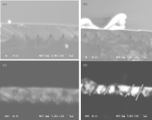
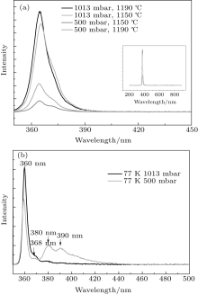
The CL is used to study the dislocation and stack fault distribution. The dark lines indicate the dislocation connection location.[12] A lot of dislocations exist in the coalescence location, as illustrated in Fig. 3(d). The dislocation and stack fault will be generated when two stripes merge during growth, because a tilt exists between the grain and the stripes. The dislocation and stack faults continue to propagate perpendicular to the c axis, and then extend to the surface. In the internal of the stripes, the dislocation is seldom observed. The dislocation density between the stripes is drastically decreased under the HP condition. The optical property is measured by the photoluminescence. When the sample is grown under the HP condition, the light emission intensity is nearly three times larger than that grown under the LP condition. The full spectrum is shown in the inset of Fig. 4. Only near band emission appears. It means that the crystal quality is very good. As shown in Fig. 4(a), except the sample grown with HP and at the temperature of 1190 ° C, one shoulder peak appears at 375 nm. Some papers have reported that this shoulder originates from the dislocation and stack faults due to the coalescence of the strips.[13] The PL result is consistent with the results of CL. Under the HP growth condition, dislocations and stack faults decrease. Hiramtsu investigated the growth mode variation by changing pressure and temperature.[14] The temperature and pressure affect the relative growth rates of the facets. The {1-101} plane is N terminal facets. At low pressure and low temperature, a lot of swollen triangles appear in the surface. These swollen triangles consist of (10-11), (0-111), and (0001) facets. When the temperature is increased, the number of swollen triangles decreases because the {1-101} surface nitrogen atoms become unstable at high temperature. By increasing the pressure, it is also found that the swollen triangles decrease. We speculate that the higher lateral growth rate of GaN is higher than the vertical growth rate. Another reason maybe H etching the N terminal {1-101} surface, so these facets are unstable and decompose seriously under the high temperature and high pressure condition. As shown in Fig. 3(d), the cross-section CL images illustrate that the LP growth sample has a distinct dark line between the stripes join position after coalescing. The distinct dark line disappears for the samples grown with HP. The obvious different features may result from the difference in the growth mode. According to the CL and the cross-section SEM, there may be two growth modes. Before the stripe coalescence, nearly all the stripes have a trapezoid cross-section. For the samples grown with pressure of 500 mbar, dislocations and stack faults extent along the [00-11] direction and fix at the (000-1) facet in the LP growth sample. Some researchers have also observed this phenomenon by TEM.[15] Even after coalesced, those dislocations and stack faults are also along the [00-11] direction and a lot of new defects are generated in the interface between two joined strips, as shown in Fig. 5(a). Those defects extend to the surface and do not decrease with increasing the thickness. The (0001) facet is Ga terminated facet and the (000-1) facet is N terminated facet. Many researchers have also found that a lot of dislocations and stack faults appear in the interface of the Ga-plane and the N-plane in non-polar GaN.[16] Another explaination is that two contact crystals have the same crystal orientation and crystal axis, two adjacent crystals should coalesce so that they may form a single domain. Unfortunately, we could not have perfect coalescence and a lot of stack faults are generated.[17] The HP growth mode is quite different. In Fig. 4(c), a lot of voids are found in the corss-section SEM. As the cross-section CL shown, the dislocation and stack fault do not gather along the [00-11] direction and fix at the interface of (000-1) and (0001) facets. We speculate the following growth mode. The growth along the [-1012] direction is much faster than that along the [10-11] direction, as shown in Fig. 4(c). In some positions, one strip vertical growth rate is lower than that of two side strips. When they connect, the (-1011) facet lateral growth is very fast. So the voids are generated when the (-1011) facet meets with the other facets. The stack fault and dislocation are much reduced due to the high lateral growth rate. So after the two strips connect, the added dislocation and stack faults at the interface of the two strips are much reduced. Under the HP condition, the PL emission intensity is much higher than that of the sample grown at low pressure, as illustrate in Fig. 4(a). In the bulk GaN, the PL emission density is determined by the band gap recombination and radiative recombination. This suggests that the non-radiative recombination center concentration is larger in the LP growth samples. The growth temperature and pressure affect the carbon and oxygen impurities concentration. Compared with the low temperature PL, the emission peaks at 380.6 nm and 390.3 nm are very obvious in the low pressure sample. These two peaks are related to the stack faults and dislocations.[11] Some researchers have reported that the deep levels and nonradioactive recombine centers are related to the C, O impurities and complexes.[18, 19]
Fig. 3. (a) Cross-section SEM and (b) CL image of samples grown at 1013 mbar and 500 mbar. (b) Cross-section SEM and (d) CL image of the sample grown at 500 mbar. In panel (d), the red bars indicate that a lot of dislocations and stack faults gather in the strips connection location.
Fig. 5. (a) Proposed growth mode of (10-11) GaN growth at 500 mbar, the dark line is the dislocation and the stack defects between the two strips connect position. (b) Proposed mode for (10-11) GaN growth at 1013 mbar. (c) Enlarged cross-section SEM image for the growth at 1013 mbar.
4. Conclusion
Growth of (10-11) GaN on patterned Si substrates under different pressures has been investigated. The coss-section SEM and CL show that the growth mode is affected by the pressure. Under the LP growth condition, the dislocation and extended stack faults gather in the interface between (0001) and (000-1) facets. Under the HP condition, after the strips connect, the dislocation and stack fault are much less. The room temperature PL results show that the PL emission intensity of the sample grown at the HP condition is three times larger than that grown at the LP condition. The PL measurement at 77 K shows that the defect-related peaks 380.6 nm and 390.3 nm are much stronger in the low pressure sample. This means the crystal quality is improved in HP growth conditions.
WuZ H, TanikawaT, MuraseT, FangY Y, ChenC Q, HondaY, YamaguchiM, AmanoH and SawakiN2011Appl. Phys. Lett. 98051902DOI:10.1063/1.3549561[Cited within:1][JCR: 3.794]
16
NiX, ÖzgürÜ, FuY, BiyikliN, XieJ, BaskiA A, MorkoçH and Liliental-WeberZ2006Appl. Phys. Lett. 89262105DOI:10.1063/1.2423328[Cited within:1]
NakanoY, IrokawaY and TakeguchiM2008Appl. Phys. Express1091101DOI:10.1143/APEX.1.091101[Cited within:1][JCR: 2.731]
19
ArmstrongA M, CrawfordM H and KoleskeD D2014Appl. Phys. Express7032101DOI:10.7567/APEX.7.032101[Cited within:1][JCR: 2.731]
1
1997
1.067
0.0
... IntroductionAlthough GaN has been widely used in electronic and optical devices,[1#cod#x2013 ...
1
2001
3.794
0.0
... [2,4] This effect restricts the carrier recombination efficiency, reduces the oscillator strength, and induces a red-shift in photon emission ...
1
2002
1.067
0.0
... 3] the conventional c-plane optical devices still suffer from the quantum-confined Stark effect (QCSE) due to the spontaneous and piezoelectric polarization fields parallel to the [0001] direction ...
2
2011
1.552
0.0
... [2,4] This effect restricts the carrier recombination efficiency, reduces the oscillator strength, and induces a red-shift in photon emission ...
... [4,5] ...
1
2011
2.731
0.0
... [4,5] ...
1
2007
1.552
0.0
... [6] However, there are still several problems in the growth of GaN on the Si substrates ...
1
2002
1.846
0.0
... [7] One of the approaches to solve these problems is to use patterned Si substrates for selective area growth (SAG) and epitaxial lateral over growth (ELO) ...
1
1999
0.0
0.0
... [8,9] High quality semi-polar GaN has been obtained by epitaxial growth on patterned Si substrates ...
2
1999
0.0
0.0
... [8,9] High quality semi-polar GaN has been obtained by epitaxial growth on patterned Si substrates ...
... [10,11] Despite the previous studies,[9,10] the effect of pressure on the (10-11) GaN quality and growth mode base on the patterned Si substrates has not been reported yet ...
2
2002
1.552
0.0
... [10,11] Despite the previous studies,[9,10] the effect of pressure on the (10-11) GaN quality and growth mode base on the patterned Si substrates has not been reported yet ...
... [10,11] Despite the previous studies,[9,10] the effect of pressure on the (10-11) GaN quality and growth mode base on the patterned Si substrates has not been reported yet ...
2
2009
1.552
0.0
... [10,11] Despite the previous studies,[9,10] the effect of pressure on the (10-11) GaN quality and growth mode base on the patterned Si substrates has not been reported yet ...
... [11] Some researchers have reported that the deep levels and nonradioactive recombine centers are related to the C, O impurities and complexes ...
1
1.067
0.0
... [12] A lot of dislocations exist in the coalescence location, as illustrated in Fig ...
1
2007
0.0
0.0
... [13] The PL result is consistent with the results of CL ...
1
1999
0.0
0.0
... [14] The temperature and pressure affect the relative growth rates of the facets ...
1
2011
3.794
0.0
... [15] Even after coalesced, those dislocations and stack faults are also along the [00-11] direction and a lot of new defects are generated in the interface between two joined strips, as shown in Fig ...
1
2006
0.0
0.0
... [16] Another explaination is that two contact crystals have the same crystal orientation and crystal axis, two adjacent crystals should coalesce so that they may form a single domain ...
1
2002
0.0
0.0
... [17] The HP growth mode is quite different ...
1
2008
2.731
0.0
... [18,19] ...
1
2014
2.731
0.0
... [18,19] ...
Effect of pressure on the semipolar GaN (10-11) growth mode on patterned Si substrates*
[Liu Jian-Minga)†, Zhang Jiea), Lin Wen-Yua), Ye Meng-Xina), Feng Xiang-Xua), Zhang Dong-Yana), Steve Dinga), Xu Chen-Kea), Liu Bao-Linb)]


 , Zhang Jie