Chen Rui, Han Jian-Wei, Zheng Han-Sheng, Yu Yong-Tao, Shangguang Shi-Peng, Feng Guo-Qiang, Ma Ying-Qi. Comparative research on “high currents” induced by single event latch-up and transient-induced latch-up* . Chinese Physics B, 2015, 24(4): 046103
Permissions
Comparative research on “high currents” induced by single event latch-up and transient-induced latch-up*
Chen Ruia),b)†, Han Jian-Weia), Zheng Han-Shenga),b), Yu Yong-Taoa),b), Shangguang Shi-Penga), Feng Guo-Qianga), Ma Ying-Qia)
National Space Science Center, Chinese Academy of Sciences, Beijing 100190, China
University of Chinese Academy of Sciences, Beijing 100049, China
*Project supported by the National Natural Science Foundation of China (Grant No. 41304148).
Abstract
By using the pulsed laser single event effect facility and electro-static discharge (ESD) test system, the characteristics of the “high current”, relation with external stimulus and relevance to impacted modes of single event latch-up (SEL) and transient-induced latch-up (TLU) are studied, respectively, for a 12-bit complementary metal–oxide semiconductor (CMOS) analog-to-digital converter. Furthermore, the sameness and difference in physical mechanism between “high current” induced by SEL and that by TLU are disclosed in this paper. The results show that the minority carrier diffusion in the PNPN structure of the CMOS device which initiates the active parasitic NPN and PNP transistors is the common reason for the “high current” induced by SEL and for that by TLU. However, for SEL, the minority carrier diffusion is induced by the ionizing radiation, and an underdamped sinusoidal voltage on the supply node (the ground node) is the cause of the minority carrier diffusion for TLU.
The latch-up in bulk complementary metal– oxide semiconductor (CMOS) integrated circuits is related to PNPN structure formed by parasitic NPN and PNP bipolar transistors. These parasitic structures are inherent to bulk CMOS, and if the latch-up is triggered in a manner which causes high current, the circuit behavior can be disturbed. In general, the latch-up includes a single event latch-up (SEL) and transient-induced latch-up (TLU) due to different external stimulus. The SEL is an event in which a single-particle interaction with a semiconductor chip can lead to latch-up. It can be initiated by a wide range of particle types. TLU means a latch-up event initiated by a fast transient triggering mode. In this paper, the triggering mode of TLU is electro-static discharge (ESD).
Numerous studies have now been done on SEL and TLU.[1– 4] The damage mode and hardening strategies of SEL and TLU have been developed, respectively.[5– 7] Although the SEL and TLU show similar responses to “ high current” , it is still not sure whether there are any correlations between the “ high current” ignited by SEL and that by TLU. Many researchers have shown great concern about the sensitivities of SEL and TLU as technology scales, while ignoring the comparative study between them.[8] It is a pity that SEL and TLU are still studied and applied separately. The possible correlation between them is unknown. More and more large-scale devices show both SEL and TLU in space radiation environment.[9, 10] In this case, it is significant to study the similarities and differences between the “ high current” induced by SEL and TLU in order to take appropriate mitigation measures.
In this work, we propose to select the 12-bit CMOS analog-to-digital converters (ADCs), AD7888 as representative samples to study the characteristics of the “ high current” , relation to external stimulus and relevance to impact modes of SEL and TLU, respectively. In general, it is desired that the similarities and differences of the physical mechanism between “ high current” induced by SEL and that by TLU can be disclosed.
2. Experimental method and samples
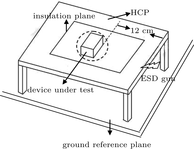
The SEL and TLU radiation experiments of AD7888 are performed at the pulsed laser single event effect facility[11] and ESD test system, respectively, in the National Space Science Center of China. The key parameters of the pulsed laser are as follows: wavelength 1.064 μ m, pulse width 25 ns, the spot size 2 µ m∼ 3 µ m, pulse repetition frequency 1 kHz∼ 50 kHz, equivalent linear energy transfer (LET) 0.1 MeV· cm− 2/mg∼ 200 MeV· cm− 2/mg. Figure 1 shows the measurement setup of the ESD testing with the indirect contact-discharge test mode, which consists of the horizontal coupling plane (HCP), insulation plane, and ESD gun. The ESD test follows the international standard (IEC 6100-4-2). When the ESD gun zaps to the horizontal coupling plane, the device under test (DUT) will be disturbed due to the high ESD-coupled energy (see Fig. 1). The discharge mode of the ESD test system is a single discharge. The discharge voltage is varied from 500 V to 20 kV.
Three 12-bit CMOS ADCs (AD7888 manufactured by AD) with the same batch are chosen. An operating voltage of 5 V is applied to the test device. The substrate depth of AD7888 is about 220 μ m. Plastic package and metal opacity are very difficult issues because they prevent the laser beam from reaching the sensitive areas of SEL. The metal layers cover a large part of the front side of AD7888. Consequently, a backside laser test should be adopted at the silicon layer after etching.
3. Experimental results and discussion
3.1. Parameter changes before and after radiation
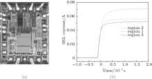
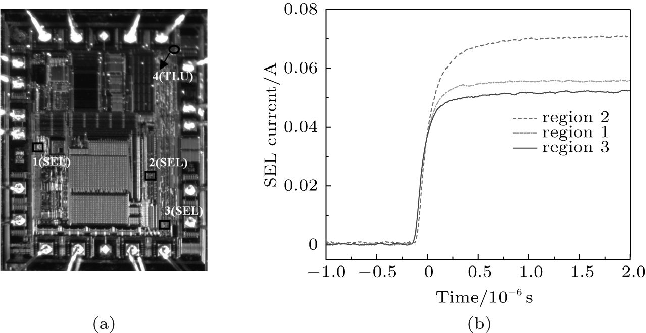
The test devices are irradiated by a pulsed laser with 13-nJ energy and 5-mm/s scanning speed. The sensitive areas of SEL for AD7888 are shown in Fig. 2(a), and the SEL currents varying with time in different regions are shown in Fig. 2(b). There are three independent regions (each is marked with a black rectangle in Fig. 2(a)), which are very sensitive to SEL. When these regions are irradiated by laser, respectively, the SEL currents of devices all increase rapidly within about 250 ns (the SEL current increases from 4 mA to 60 mA for region 1, the SEL currents of region 2 and region 3 increase up to 71 mA and 55 mA respectively), as shown in Fig. 2(b).
Fig. 2. Sensitive regions of SEL and TLU (a) and the changes of SEL current with time (b) in different regions of AD7888.
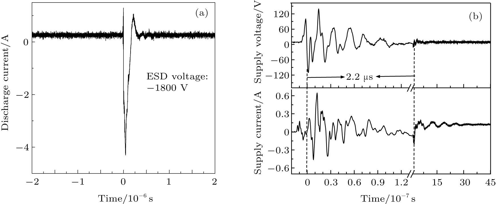
The sensitive area of TLU (region 4, marked with a black circle) for AD7888 is also shown in Fig. 2(a) by the ESD testing. The changes of supply voltage and current of the test devices with time under ESD voltages of 500 V and – 1800 V are shown in Fig. 3 and Fig. 4, respectively. No matter which ESD voltage is applied: 500 V or – 1800 V, the variations of supply voltage and
Fig. 4. Changes of discharge current (a) and supply voltage and current (b) with time for the test device under an ESD voltage of – 1800 V.
current of the test device with time clearly show underdamped sinusoidal oscillation.[6] When the ESD voltage is 500 V, the transient discharge current is as large as about 1.7 A and the transient peak voltage and current are greater than 30 V and 200 mA, respectively. Clearly, the supply voltage with initial + 5 V will become an underdamped sinusoidal voltage due to the disturbance of the ESD energy. When the ESD voltage keeps increasing, the TLU can be initiated and the TLU current will instantaneously increase to 119 mA. The damping times of supply voltage and current of the test device are both about 0.18 µ s, as shown in Fig. 3(b). With an ESD voltage of – 1800 V, the measured transient waveforms of discharge current, supply voltage, and supply current are similar to those in Fig. 3. The peaks of transient discharge current, supply voltage, and supply current are greater than – 4 A, 120 V, and 600 mA, respectively, as shown in Fig. 4. The damping time observed in Fig. 4(b) is about 2.2 µ s, and the TLU current is still 119 mA.
3.2. Discussion
3.2.1. Latch-up current
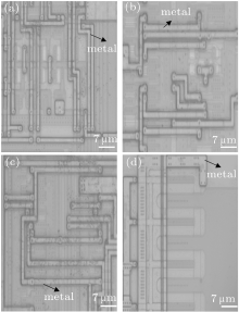
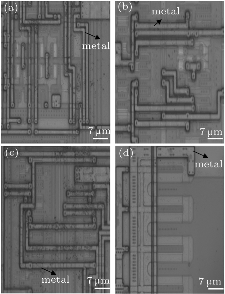
The latch-up current is a visual characteristic of SEL and TLU effect. The amplitude of latch-up current reflects the sensitivities of the responses to SEL and TLU effect. To investigate the difference between “ high current” induced by SEL and that by TLU, 1000-times enlarged photographs of the sensitive areas of SEL and TLU (which are shown in Fig. 2(a)) are shown in Fig. 5. The analysis of the extracted layout shows that the three sensitive areas of SEL all belong to the logical circuits and the sensitive area of TLU is the input/output (I/O) cell for AD7888.
According to the layout rule of CMOS process, the sizes of transistor in an I/O circuit is larger than that in a logical circuit, and the equivalent resistance of an I/O circuit is smaller than that of a logical circuit in most cases. Numerous studies show that the size of transistor and equivalent resistance in PNPN structure are directly related to the sensitivity of the latch-up.[12– 15] In general, the PNPN structure formed by the larger size of transistor needs a higher triggering energy of the latch-up. In addition, because of the smaller equivalent resistance in an I/O circuit, the latch-up current induced by TLU (119 mA) is larger than those induced by SEL (71 mA, 60 mA, and 54 mA) in the same test device.
Fig. 5. The 1000 times enlarged photographs of the sensitive areas of region 1 (a), region 2 (b), region 3 (c), and region 4 (d).
3.2.2. Latch-up holding voltage
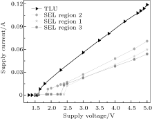
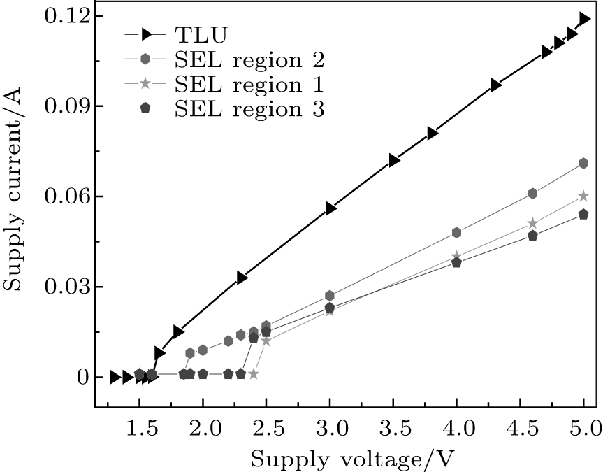
The latch-up holding voltage is the voltage in a low-voltage/high-current state that first occurs during latch-up. When the supply voltage of the test device is higher than the latch-up holding voltage, the latch-up effect of the test device occurs. The changes of the supply current with the supply voltage for SEL (incidence region 1, incidence region 2, and incidence region 3) and TLU in AD7888 are shown in Fig. 6.
Fig. 6. Changes of the supply current with the supply voltage for SEL and TLU.
When the supply voltage of the test device decreases from its normal operating voltage (5 V) to 2.4 V, the supply current of region 1 decreases from 60 mA down to 1 mA. With a further decrease from 2.4 V to 2.3 V, the supply current of region 3 is reduced from 13 mA to 1 mA. The supply current of region 2 is reduced from 8 mA to 1 mA while the supply voltage further decreases to 1.85 V. Therefore, the test device that is shot at each sensitive position would be released from SEL when the supply voltage of the test device is reduced down to 1.85 V. However, for the supply current of the test device induced by TLU, the supply current is reduced from 8 mA to 0 mA while the supply voltage of the test device is lower than 1.65 V. The test device is free from TLU at this moment. Many researchers[2– 5] have shown that there is a relationship between latch-up holding voltage and the sensitivity of latch-up effect for CMOS technology. As the latch-up holding voltage decreases, the sensitivity of latch-up effect increases. Therefore, it is found that TLU is much easier to trigger for the test device.
3.2.3. Relationship with the external stimulus
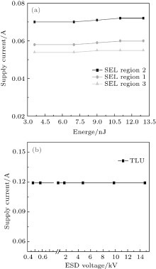
The changes of the SEL and TLU current with external stimulus are shown in Fig. 7. With an ESD voltage of 500 V, TLU is triggered and the TLU current is 119 mA in CMOS AD7888. However, with an ESD voltage of 1.5 × 10⁴ V, the TLU current is still 119 mA, as shown in Fig. 7(a). A similar result is shown in Fig. 7(b). As the laser energy increases from 3.6 nJ to 13 nJ, the SEL current of the test device keeps constant (the SEL currents of region 1, region 2, and region 3 are 60 mA, 71 mA, and 55 mA, respectively).
From Fig. 7, it is found that neither the SEL current nor TLU current can be influenced by changing the stimulation mode (increasing the ESD voltage or laser energy) as the latch-up effect of the test device is triggered. Some reports[8] have shown that the collector-emitter voltage of the parasitic bipolar transistor decreases due to the increase of the voltage of the load resistance because the latch-up current is large. Because of the decrease of collector-emitter voltage of the parasitic bipolar transistor, the operating mode of the test device is changed from the amplification state to saturation state, which finally causes the saturation of the latch-up current. This may explain why SEL current and TLU current are independent of the change of external stimulation.
Fig. 7. Changes of SEL (a) and TLU (b) current of the test device with external stimulus.
3.2.4. Impacted mode
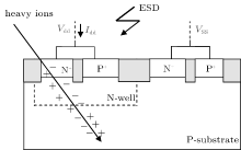
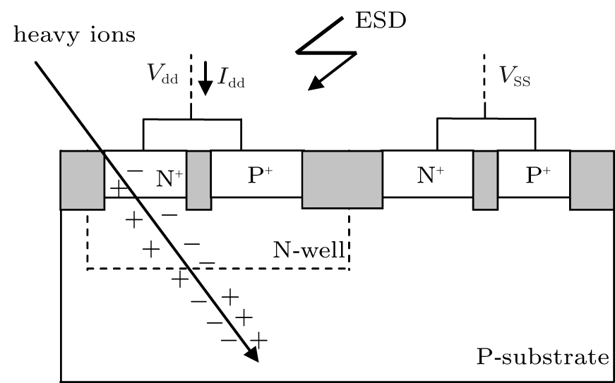
The impacted modes of SEL effect and TLU effect in CMOS PNPN structure are shown in Fig. 8. Under the normal operating condition, the anode (Vdd) and the cathode (Vss) of the PNPN structure are isolated by a reverse biased well-substrate junction and only a small leakage current of the diode flows between them.
In a heavy ion event, the heavy ion can interact with a CMOS PNPN structure. Many electron– hole pairs are generated in the process, as shown in Fig. 8. Because of the reverse biased well-substrate junction, a large number of the minority carriers drift from N-well region to substrate, which makes the potential of N-well decrease and the potential of substrate increase.[9] When the potential difference between them reaches a certain level (> 0.7 V), the lateral transistor formed by N+ -source, P-substrate, and N-well is activated, and likewise, the vertical transistor formed by P+ -source, N-well, and P-substrate is also activated due to the falling N-well potential. When the two parasitic transistors are activated simultaneously, a regenerative feedback between the parasitic npn and the pnp is formed, as shown in Fig. 5. As a result, SEL eventually occurs.
Fig. 8. Schematic diagram of the impacted modes of SEL and TLU.
However, the impacted mode of TLU is different from that of SEL. When the electromagnetic pulse caused by ESD impacts the Vdd node (Vss node) of the PNPN structure, an underdamped sinusoidal voltage will be generated, which is shown in Fig. 3 and Fig. 4. Taking Fig. 3(b) for example, the measured transient responses of the supply voltage and current can be divided into several parts for a detailed discussion in the time domain. Firstly, during the period of 0 < t ≤ 2 ns, the supply voltage begins to decrease rapidly from its normal operating voltage (5 V) and will eventually reach a negative peak voltage of − 8 V at t = 2 ns. The potential difference between the N-well and P-substrate decreases gradually with supply potential decreasing from 5 V to 0 V. When the potential difference between them is lower than − 0.7 V, the PN junction transistor formed by N-well and P-substrate is activated. Hence, a lot of minority carriers in the N-well region are injected into the substrate, which causes the supply current to negatively increase. Secondly, during the period of 2 ns < t ≤ 7 ns, the supply voltage increases from the negative peak voltage to the forward peak voltage (25 V). At this time, the N-well/P-substrate junction will rapidly change from the forward-biased state to its original reverse-biased state. Meanwhile, inside the N-well region, a large number of stored minority holes offered by the forward peak current at t = 7 ns, will be instantaneously swept back to the P-substrate region where they originally come from.[7] Thus, such a sweep-back current will produce a localized voltage drop while flowing through the parasitic N-well or P-substrate resistance. Once this localized voltage drop approaches to some critical value, the parasitic pnp and npn transistors will be activated, and then TLU is triggered.
Based on the above analysis, it can be clarified that the minority carrier diffusion induced by irradiation in a PNPN structure is a major impacted mode of SEL. For TLU characterization, an underdamped sinusoidal voltage caused by ESD on the Vdd node (Vss node) of the PNPN structure is identified as a major cause.
4. Conclusions
In this paper, the response characteristics of SEL and TLU effect for CMOS AD7888, including the characteristics of the “ high current” , relation with external stimulus and relevance to impacted mode, are studied. It is demonstrated that it is more sensitive to TLU for the CMOS AD7888 by making a comparison of the holding voltage between SEL and TLU. Once SEL or TLU is triggered, the latch-up current is irrelevant to the external stimulus.
What is more, the minority carrier diffusion which causes the active parasitic npn and pnp transistors in PNPN structure is the potential impacted mode of SEL and TLU. However, the different reasons which initiate the minority carrier diffusion between SEL and TLU are the main differences. For the impacted mode of SEL, the changes of N-well and P-substrate potential, caused by the heavy ions, are the major cause of the minority carrier diffusion. But the underdamped sinusoidal voltage induced by ESD on the Vdd node (Vss node) of the PNPN structure can result in the minority carrier diffusion for TLU impact.
VoldmanS H, GebreselasieE, ZierakM, HershbergerD, CollinsD, FeilchenfeldN, OngeS St and DunnJ2005Proceedings of the 43th Annual International Reliability Physics SymposiumApril 17–212005, San Jose, USA129[Cited within:1]
5
DoddsN A, HootenN C, ReedR A, SchrimpfR D, WarnerJ H, RocheN J H, McMorrowD, WenS J, WongR, SalzmanJ F, JordanS, PellishJ A, MarshallC J, GaspardN J, BennettW G, ZhangE X and BhuvaB L2012IEEE Trans. Nucl. Sci. 592642[Cited within:2]
SukhaseumN, SamarasA, DuD L, Vand eveldeB, ChatryN and BezerraF2012Proceedings of the 13th European Conference on Radiation and Its Effects on Components and SystemsSeptember 24–28, 2012Biarritz, France[Cited within:1]
14
DoddsN A2012“Single event latchup hardening strategies, trigging mechanisms, and testing considerations”Ph. D. ThesisNathanielGraduate School of Vand erbilt University[Cited within:1]
15
BurnellA J, ChuggA M and Harboe-SorensenR2010IEEE Trans. Nucl. Sci. 57[Cited within:1]
1
1979
0.0
0.0
... [1#cod#x2013 ...
1
1969
0.0
0.0
... Many researchers[2#cod#x2013 ...
1
1995
0.0
0.0
1
2005
0.0
0.0
... 4] The damage mode and hardening strategies of SEL and TLU have been developed, respectively ...
2
2012
0.0
0.0
... [5#cod#x2013 ...
... 5] have shown that there is a relationship between latch-up holding voltage and the sensitivity of latch-up effect for CMOS technology ...
1
2005
0.0
0.0
... [6] When the ESD voltage is 500#cod#x00A0 ...
2
2006
0.0
0.0
... 7] Although the SEL and TLU show similar responses to #cod#x201C ...
... [7] Thus, such a sweep-back current will produce a localized voltage drop while flowing through the parasitic N-well or P-substrate resistance ...
2
2007
0.0
0.0
... [8] It is a pity that SEL and TLU are still studied and applied separately ...
... Some reports[8] have shown that the collector-emitter voltage of the parasitic bipolar transistor decreases due to the increase of the voltage of the load resistance because the latch-up current is large ...
2
2014
1.016
1.691
... [9,10] In this case, it is significant to study the similarities and differences between the #cod#x201C ...
... [9] When the potential difference between them reaches a certain level (#cod#x003E ...
1
2012
1.148
1.2429
... [9,10] In this case, it is significant to study the similarities and differences between the #cod#x201C ...
1
2009
0.0
0.3451
... Experimental method and samplesThe SEL and TLU radiation experiments of AD7888 are performed at the pulsed laser single event effect facility[11] and ESD test system, respectively, in the National Space Science Center of China ...
1
2011
0.0
0.0
... [12#cod#x2013 ...
1
2012
0.0
0.0
1
2012
0.0
0.0
1
2010
0.0
0.0
... 15] In general, the PNPN structure formed by the larger size of transistor needs a higher triggering energy of the latch-up ...
Comparative research on “high currents” induced by single event latch-up and transient-induced latch-up*
[Chen Ruia),b)†, Han Jian-Weia), Zheng Han-Shenga),b), Yu Yong-Taoa),b), Shangguang Shi-Penga), Feng Guo-Qianga), Ma Ying-Qia)]


 , Han Jian-Wei