Improvement of the off-state breakdown voltage with field plate and low-density drain in AlGaN/GaN high-electron mobility transistors*
Zhang Peng, Zhao Sheng-Lei, Hou Bin, Wang Chong, Zheng Xue-Feng, Ma Xiao-Hua†

, Zhang Jin-Cheng, Hao Yue
Key Laboratory of Wide Band-Gap Semiconductor Materials and Devices, School of Advanced Materials and Nanotechnology, Xidian University, Xi'an 710071, China
†Corresponding author. E-mail: xhma@xidian.edu.cn
*Project supported by the Key Program of the National Natural Science Foundation of China (Grant No. 61334002) and the Young Scientists Fund of the National Natural Science Foundation of China (Grant Nos. 61404100 and 61106106).
1. IntroductionGaN-based high-electron mobility transistors (HEMTs) are excellent candidates for power electronics applications due to their superior material properties, such as high electron mobility and high energy band gap.[1] The application of GaN HEMTs is limited by the lack of a normally-off device, device cost, and reliability issues, such as current collapse. For many years breakdown character has also been a major concern of GaN device reliability in power electronics applications. The theoretical critical electric-field of GaN is 3.3 MV/cm, which is ten times higher than that of Si material.[2] So the breakdown voltage (BV) of a GaN device is supposed to be very tempting theoretically. However, the actual BV of I-gate (gate without field plate structure) HEMT is usually below 100 V, which is unacceptable in high voltage applications.[3– 5] Meanwhile, to compensate for the reduction in the maximum current and to maintain similar power handling capability in enhancement-mode devices, the BV needs to be improved without increasing the gate-to-drain distance because it inevitably increases the device size.[6]
The main reason of the low BV is that the electric field (E-field) is extremely concentrated near the gate edge due to the thin conducting channel in AlGaN/GaN hetero structures. Given that the theoretical critical electric-field of AlGaN is much higher than GaN due to the composition of Al, the GaN buffer near the hetero interface suffers early breakdown. The major solution of the breakdown issue is placing a field-plate (FP) structure above the gate edge, including gate-plate and source-plate. A lot of work has been done by Saito[7– 9] and Mishra, [10– 12] proving the prominent effect of FPs. The low potential metal plate enables the redistribution of the E-field and the reduction of the peak field.[13– 16] However, the frequency characteristic is unavoidably affected due to parasitics induced by the dielectric capacitance under the FP.[17] Meanwhile, depleting the two-dimensional electron gas (2DEG) density near the gate edge by low power fluorine (F– ) ions injection provides immobile negative charges in the AlGaN barrier and effectively depletes the electrons in the channel, which can modulate the fatal E-field peak with minimum parasitic. This method was first proposed by Song et al.[18] This low-density drain HEMT (LDD-HEMT) shows another method to enhance BV and reduce current collapse.[19, 20]
In this paper, we proposed a novel AlGaN/GaN HEMT structure with a combination of small-size gate-FP and low-power LDD structure to effectively enhance the BV. Our experimental results indicated that the proposed LDD devices exhibit a three times enhancement of off-state BV.
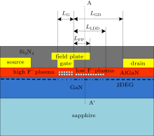
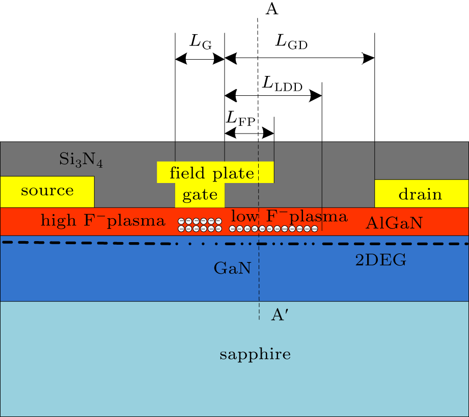
2 ExperimentThe AlGaN/GaN hetero structures were grown on a (0001) sapphire substrate in a metal organic chemical vapor deposition (MOCVD) system at Xidian University. The epitaxial layer contains a 20-nm undoped Al0.30Ga0.80N barrier layer, a 1.2-nm AlN interlayer, a 1.6-μ m unintentionally doped GaN buffer layer, and a low-temperature GaN nucleation layer. A sheet carrier density of 1.01× 1013 cm– 2, an electron mobility of 1943 cm2/(V· s), and a sheet resistance of 347 Ω /square of the hetero structures were measured using Hall effect measurements at room temperature.
The cross section of the LDD HEMT is shown in Fig. 1. The device fabrication commenced with mesa isolation using Cl2/Ar plasma dry etching in a reactive ion etching (RIE) system, followed by the source/drain ohmic contacts, consisting of Ti/Al/Ni/Au annealed in N2 ambient at 830 ° C for 30 s. The resistance of the ohmic contact is 0.37 Ω · mm. Then a CF4 plasma ion implantation with a RF source power of 100 W for 45 s was carried out in LDD area with different lengths of LDD (LLDD), followed on with deposition of a 60-nm Si3N4 passivation layer at 300 ° C by the plasma-enhanced chemical vapor deposition (PECVD) method. After that, a second CF4 plasma treatment with a power of 120 W for 60 s was applied on the gate region and was subsequently annealed at 300 ° C for 4 min to repair the plasma-induced damages. Finally, the Ni/Au/Ni Schottky gate and gate-FP was deposited by the e-beam evaporation method. Devices without LDD treatment or FP were also fabricated on the same wafer for a fair comparison. The fabricated devices have a gate– drain spacing (LGD) of 2.5 μ m, a gate-source spacing of 0.9 μ m, a gate length of 0.5 μ m, and a FP length (LFP) of 0.5 μ m, as shown in Fig. 1.
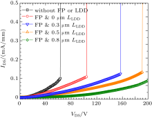
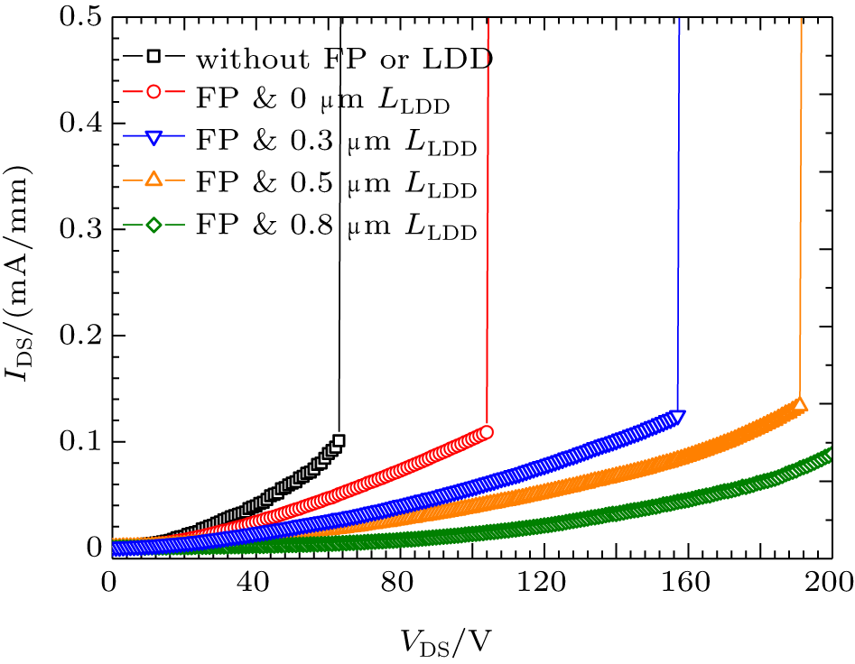
3 Results and discussionThe three-terminal off-state breakdown characteristics of the LDD MISHEMTs along with an ordinary T-gate HEMT are shown in Fig. 2. VGS was set at – 10 V to fully pinch off the devices. The breakdown measurement was carried out in air ambience. The limitation of the testing equipment is 200 V. The LDD spacing (LLDD) is designed from 0 μ m to 0.8 μ m, the device with both FP and LDD (0.8 μ m LLDD, only 31% of the LGD) achieves a BV enhancement up to two times compared with the device with only FP and three times compared with the device without FP or LDD. Although the best BV obtained was limited at 200 V, it was still far above other obtained BV in Refs. [17] and [18] with LDD treatment at almost the same gate to drain distance.
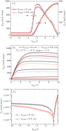
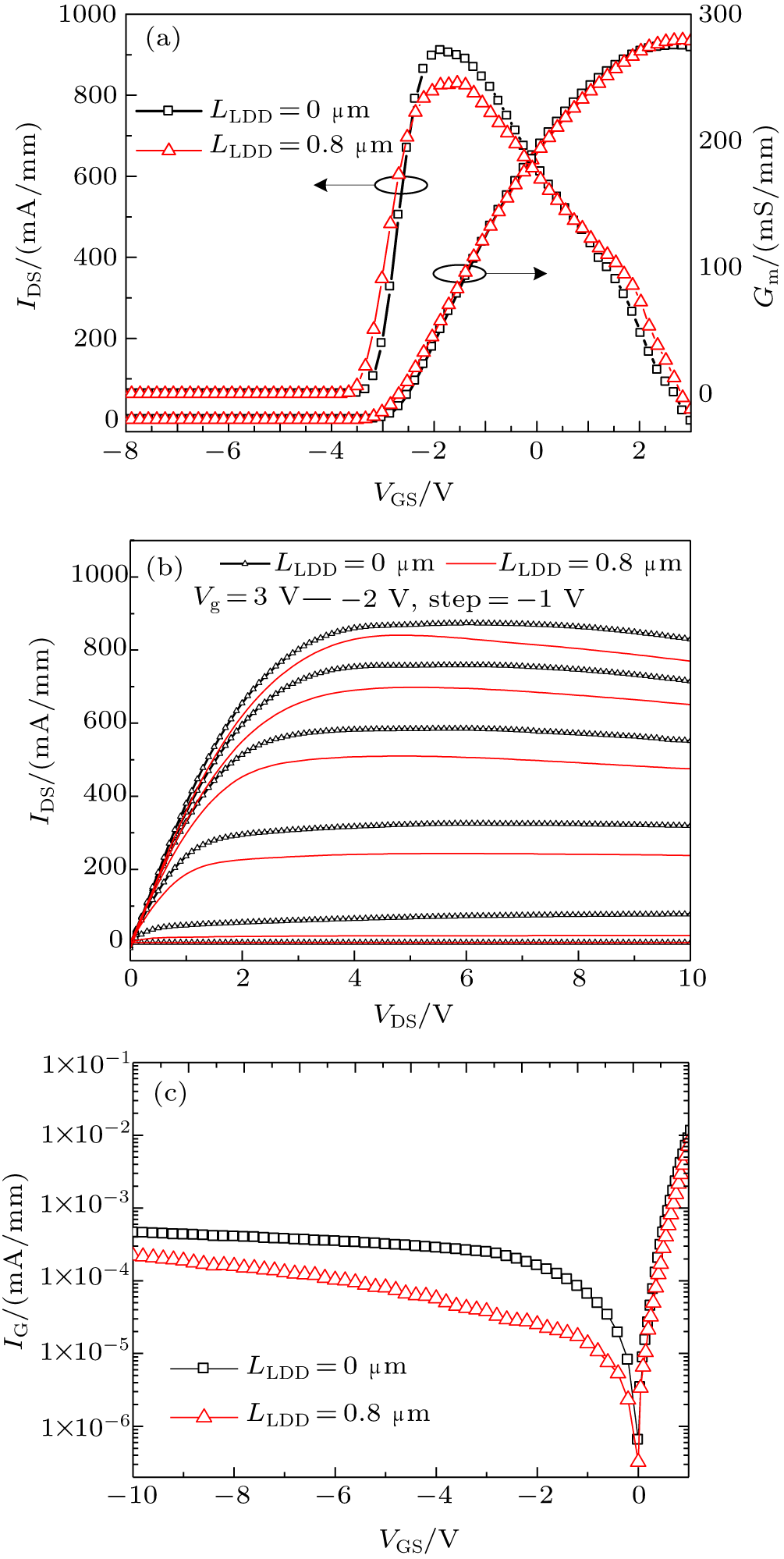
In Fig. 3(a) no obvious change in Vth and transconductance is observed because no F– ions plasma is applied on the gate region. So we believe that the LDD treatment has no influence on the transfer characteristic. The possible Vth shift can be considered as the F– ion concentration changing under the gate as a result of non-self-alignment between the two separate (the gate and the LDD) CF4 plasma treatments. In Fig. 3(b), the output current shows slight degradation caused by the immobile negative fluorine charges reducing the 2DEG density and less than a 1 V increase of Vknee is observed. In Fig. 3(c) no obvious change of gate leakage current is observed, showing that the low-power F-injection in LDD has no influence on the leakage path deep in the GaN buffer.
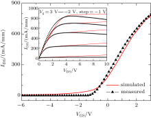
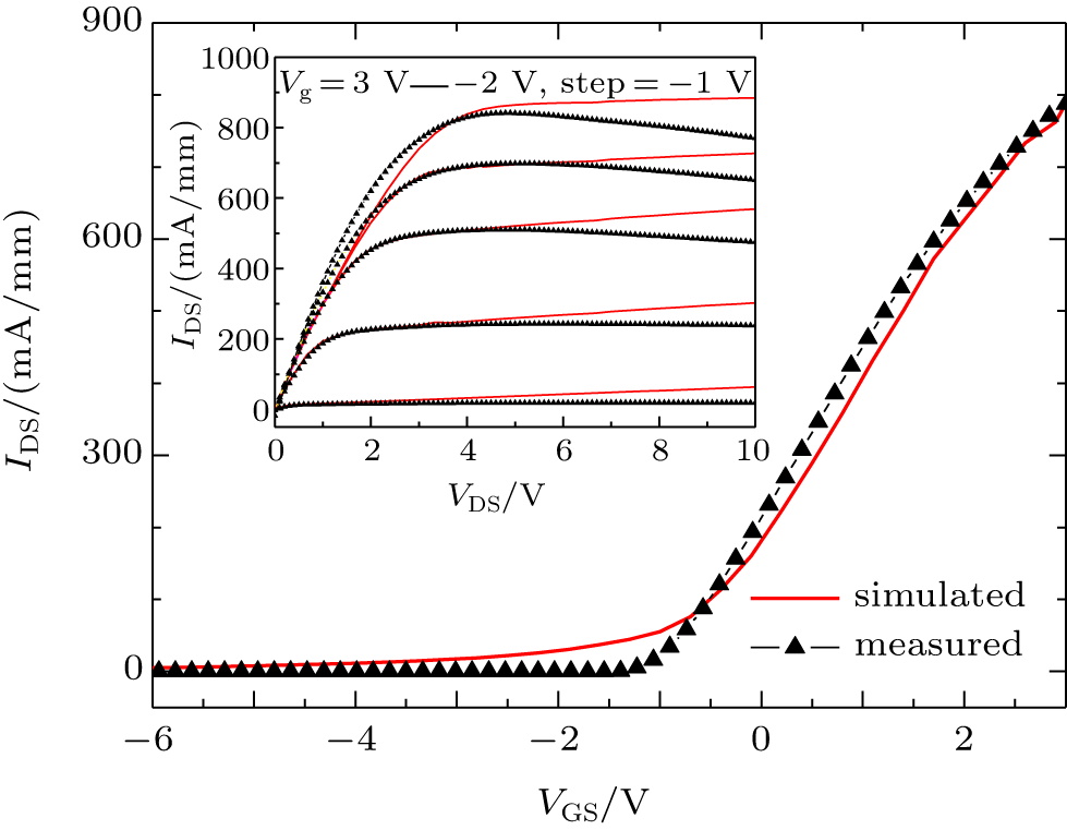
To support the above analysis, two-dimensional device simulations on GaN HEMTs using Silvaco ATLAS were also performed. The physical structure of the simulated HEMT consisted of a 20-nm AlGaN barrier layer, a 0.2-μ m GaN layer, a 0.5-μ m gate length, and a 0.5-μ m FP length, which exactly corresponds to the real geometric structure of the fabricated devices. The 2DEG areal density of 1.01× 1013 cm– 2 was chosen to fit the experimental curves in Fig. 4. Meanwhile, in order to take the CF4 plasma treatment into account, the 2DEG areal density was adjusted at 0.3× 1013 cm– 2 under the gate to give the correct threshold voltages, and 0.6× 1013 cm– 2 under the LDD area. The 2DEG mobility in the channel was set to 1943 cm2/(V· s), which is exactly equal to the actual AlGaN/GaN hetero material. The gate work function was set to 5.23 eV, corresponding to the work function of Ni as the first layer of gate metal. The other material parameters were the same as those used in Ref. [21].
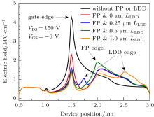
Figure 4 presents the measured transfer (IDS– VGS) and output (IDS– VDS) characteristics along with simulation curves for AlGaN/GaN HEMTs with both 0 μ m and 0.8 μ m LLDD. The simulation curves are in accord with the experimental results. After that, by using this well-fitted device structure, we preformed simulation of E-field distribution of the LDD devices at VDS of 150 V and VGS of – 6 V, as shown in Fig. 5. The normal device without LDD and FP shows its electric field peak up to 4 MV/cm, , which is beyond the GaN limit, so the actual BV of this device must be below 150 V. Meanwhile, the simulated electric field peak of LDD-HEMT is effectively reduced, revealing the reason for the BV enhancement in the experimental results. It is known that FP can efficiently ease the E-field peak near the gate edge by changing it into two lower peaks (the other is near the FP edge). The LDD further modulates the E-field into three peaks (the third is near the LDD edge) with an even lower concentration value. The device with both FP and 1.0-μ m LDD showed the lowest electric field peak. Thus, the device with both FP and LDD is the least likely to reach the critical E-field of GaN material and achieved the highest BV.
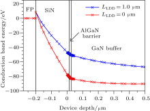
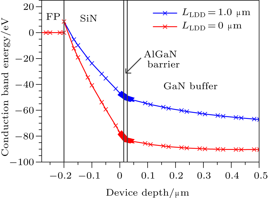
According to Ref. [22], F– ions as negatively immobile charges cause an upward bending of the conduction band and lead to an increase in Schottky barrier height. The simulated conduction band energy of the AlGaN/GaN hetero structures along the cross section of AA' in Fig. 1 is shown in Fig. 6. This proves that the LDD treatment raised the conduction band energy. This enhanced band energy depletes the channel electrons and causes a relieved E-field density in the LDD area.
4 ConclusionBy using both the field plate and the F– ions injection in the LDD area, we have demonstrated an AlGaN/GaN HEMT with modified off-state breakdown behaviors. The obvious effect of BV enhancement was achieved without device degradation. The BV is far above other works with LDD treatment, in spite of testing equipment limitation. By using two-dimensional device simulations, the mechanism of the LDD treatment was supposed to be an enhanced band energy and depleted channel electrons in the LDD area, leading to modified E-field distribution and increased BV of the device.


