
Trap states induced by reactive ion etching in AlGaN/GaN high-electron-mobility transistors*
[Luo Juna) , Zhao Sheng-Leia) , Mi Min-Hana) , Hou Binb) , Yang Xiao-Leib) , Zhang Jin-Chenga) , Ma Xiao-Huaa), b) , Hao Yuea)  ]
]
]
|
|


†Corresponding author. E-mail: yhao@xidian.edu.cn
*Project supported by the National Natural Science Foundation of China (Grant Nos. 61334002 and 61106106).
Frequency-dependent conductance measurements were carried out to investigate the trap states induced by reactive ion etching in AlGaN/GaN high-electron-mobility transistors (HEMTs) quantitatively. For the non-recessed HEMT, the trap state density decreases from 2.48 × 1013 cm−2·eV−1 at an energy of 0.29 eV to 2.79 × 1012 cm−2·eV−1 at ET = 0.33 eV. In contrast, the trap state density of 2.38 × 10¹³–1.10 × 1014 cm−2·eV−1 is located at ET in a range of 0.30–0.33 eV for the recessed HEMT. Thus, lots of trap states with shallow energy levels are induced by the gate recess etching. The induced shallow trap states can be changed into deep trap states by 350 °C annealing process. As a result, there are two different types of trap sates, fast and slow, in the annealed HEMT. The parameters of the annealed HEMT are ET = 0.29–0.31 eV and DT = 8.16 × 10¹²–5.58 × 1013 cm−2·eV−1 for the fast trap states, and ET = 0.37–0.45 eV and DT = 1.84 × 10¹³ − 8.50 × 1013 cm−2·eV−1 for the slow trap states. The gate leakage currents are changed by the etching and following annealing process, and this change can be explained by the analysis of the trap states.
GaN-based high-electron-mobility transistors (HEMTs) have attracted a lot of attention for high-frequency and high-power applications due to their excellent material and device performance.[1– 3] Recessed-gate GaN-based HEMTs and MISHEMTs are desirable to realize the normally-off operation to reduce power consumption and simplify circuit configuration.[4– 6] In addition, recessed-gate structure could increase the maximum transconductance and enhance the frequency performance.[7] To realize the recessed-gate structure, the gate recess etching technique is widely used based on Cl2-based inductively-coupled plasma reactive ion etching (ICP-RIE) process.[4– 6] However, trap states would be induced by the gate recess etching process, leading to a larger gate leakage, lower breakdown voltage, and worse current collapse characteristic.[8– 10] Although a lot of research papers have investigated the effects of the gate recess etching on dc and current collapse characteristics of the AlGaN/GaN HEMTs, the etching-induced trap states in the AlGaN/GaN HEMTs have hardly been investigated quantitatively.
Frequency-dependent conductance measurements are utilized widely to analyze the trap states in GaN-based HEMTs.[11, 12] In this paper, the trap states induced by reactive ion etching (RIE) in AlGaN/GaN HEMTs have been investigated by frequency-dependent conductance measurements. 350 ° C annealing process was performed to investigate the effect of post-gate annealing on the trap states. Besides, the variation of the gate leakage current has been discussed through the analysis of the trap states.
The AlGaN/GaN heterostructure was grown on a 2-in sapphire substrate by the metal-organic chemical vapor deposition (MOCVD). The epitaxial layers consist of a 140-nm AlN nucleation layer, a 1.4-μ m GaN buffer layer, and a 22-nm Al0.30Ga0.70N barrier layer. The first step of the device fabrication was to anneal the e-beam evaporated Ti/Al/Ni/Au at 830 ° C for 30 s to realize the ohmic contact. Then, mesa isolation was performed by reactive ion etching with Cl2. All the devices were passivated with 60-nm SiN to eliminate the effect of surface states. For the recessed-gate HEMT, a Cl2-based RIE was performed to reduce the gate-to-channel distance to 13.8 nm after etching the top SiN passivation using F-based plasma. The metal stack of Ni/Au was deposited to form the Schottky gate. Figure 1 shows the cross-sectional view of the recessed-gate AlGaN/GaN HEMT. All the HEMTs tested have a gate length LG = 1.0 μ m, a gate– source spacing LGS = 0.8 μ m, and a gate– drain spacing LGD = 1.2 μ m. Circular shaped Schottky barrier diodes (SBDs) were utilized for frequency-dependent conductance measurements with a circular gate contact having a diameter of 130 μ m and surrounding ohmic contact with an ohmic-Schottky separation of 30 μ m. After dc and C– V measurements, the recessed-gate HEMTs were annealed at 350 ° C for 10 min in N2 ambient to study the effects of post-gate annealing on recessed-gate HEMTs.
 | Fig. 1. Schematic structure of the recessed-gate AlGaN/GaN HEMT. |
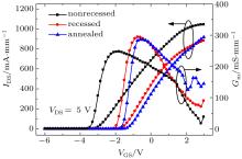
Figure 2 shows the transfer characteristics of the nonrecessed AlGaN/GaN HEMT, recessed-gate AlGaN/GaN HEMT, and annealed AlGaN/GaN HEMT at VDS = 5 V. The threshold voltage Vth shifts from − 2.9 V to − 1.5 V as a result of the gate recess etching. Due to a shorter gate-to-channel distance, the maximum transconductance increases from 247 mS/mm of the nonrecessed HEMT to 294 mS/mm of the recessed-gate HEMT. The maximum drain current of the recessed HEMT is 882 mA/mm at VGS = 3 V. 30 recessed HEMTs distributed in the wafer were measured before and after post-gate annealing, and it is found that the transconductance and the maximum drain current of the recessed HEMT are hardly changed by post-gate annealing. The positive threshold voltage shift (0.1– 0.3 V) has been observed in all the HEMTs, and the Vth of the recessed HEMT as shown in Fig. 2 shifts from − 1.5 V to − 1.34 V.
 | Fig. 2. Transfer characteristics of the nonrecessed AlGaN/GaN HEMT, recessed-gate AlGaN/GaN HEMT, and annealed AlGaN/GaN HEMT at VDS = 5 V. The annealed HEMT refers to the recessed-gate HEMT treated by post-gate annealing at 350 ° C for 10 min. |
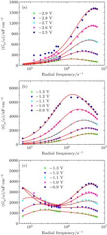
The conductance measurements in the frequency range from 10 kHz to 1 MHz were used to characterize the trapping effects in the three HEMTs. Figure 3 shows the equivalent parallel conductance Gp/ω as a function of radial frequency ω = 2π f for the three HEMTs at selected gate biases near the threshold voltage. Based on the gate biases, small ac measurement signal Vac is applied to the gate terminal. The frequency discussed in this paper is the frequency of Vac. There exists one Gp/ω peak in the nonrecessed HEMT and the recessed-gate HEMT. In contrast, two Gp/ω peaks are observed in the annealed HEMT, indicating that there are two kinds of trap sates in the annealed HEMT. The conductance Gp/ω for one or two kinds of trap states can be, respectively, expressed as
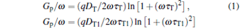 |
 |
where DT is the trap state density, τ T is the trap state time constant, Gp/ω has a maximum at ω = 2/τ T and at that maximum DT = 2.5Gp/qω .
 | Fig. 3. Conductance as a function of radial frequency for (a) nonrecessed HEMT, (b) recessed-gate HEMT, and (c) annealed HEMT at selected gate biases. Full lines are fitting curves. |
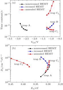
The time constant of the trap states as a function of the gate voltage evaluated for the three HEMTs is shown in Fig. 4(a). The trap state energy ET can be found by using the time constant resulting from the fitting procedure and considering that τ T = (σ TNcvT)− 1exp(ET/kT), where the capture cross section of the trap states σ T = 3.4 × 10− 15 cm− 2, the density of states in the conduction band Nc = 2.2 × 1018 cm− 3, and the average thermal velocity of the carriers vT = 2.6 × 107 cm/s were used.[12] The trap state density as a function of their energy levels is shown in Fig. 4(b).
 | Fig. 4. (a) Trap state time constant as a function of gate voltage. (b) Trap state density as a function of their energy levels. |
There is one kind of trap states (trap A) in the nonrecessed AlGaN/GaN HEMT with trap state time constant τ T = 0.38– 1.51 μ s. The trap state density DT in the non-recessed HEMT decreases from 2.48 × 1013 cm− 2· eV− 1 at an energy of 0.29 eV to 2.79 × 1012 cm− 2· eV− 1 at ET = 0.33 eV. For the recessed HEMT, a trap (trap B) state density of 2.38 × 10¹³– 1.10 × 1014 cm− 2· eV− 1 is located at ET in a range of 0.30– 0.33 eV. Thus, lots of trap states with shallow energy levels are induced by the gate recess etching. Two different types of trap sates, fast and slow, are present in the annealed HEMT. The trap state time constant is 0.42– 0.69 μ s for the fast trap states (trap C1) and 8.95– 146 μ s for the slow trap states (trap C2). The parameters of the annealed HEMT are ET = 0.29– 0.31 eV and DT = 8.16 × 10¹²– 5.58 × 1013 cm− 2· eV− 1 for the fast trap states, and ET = 0.37– 0.45 eV and DT = 1.84 × 10¹³– 8.50 × 1013 cm− 2· eV− 1 for the slow trap states.
Trap A is an intrinsic trap in AlGaN/GaN HEMT, located at the AlGaN/GaN interface. In contrast, trap B includes two parts, namely an intrinsic trap and etching induced trap. The density of the induced trap is very large compared with the intrinsic trap, and these two traps have the similar energy levels. As a result, the intrinsic trap is covered by the induced trap and is hard to be extracted by the frequency-dependent conductance measurements in the recessed HEMT. The induced trap is changed to trap C2 with deeper energy levels by annealing process, resulting in the separation of the intrinsic trap and etching induced trap. The intrinsic trap is affected by the etching and annealing process, and it becomes trap C1. In addition, the density of the trap C1 in the annealed HEMT is larger than that of the trap A in the nonrecessed HEMT.
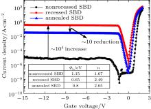
The gate leakage currents are changed by the gate recess etching and the following annealing process. Figure 5 shows the gate currents of the nonrecessed SBD, the recessed-gate SBD, and the annealed SBD. The reverse gate leakage current of the nonrecessed SBD at VGS = − 15 V is 1.37 × 10− 5 A/cm2, which is a relatively low value for AlGaN/GaN HEMTs without any gate insulator or surface treatment. The reverse leakage current increases by four orders of magnitude after gate recess etching. For the annealed SBD, the reverse leakage current is one order of magnitude lower than that of the recessed-gate SBD without annealing. The effective Schottky barrier height Φ b and the ideality factor n are extracted from the gate forward current characteristics based on the electron thermal emission (TE) model. Φ b and n are deteriorated by gate recess etching, and then improved by annealing process, as shown in the inserted table of Fig. 5. The similar variation of the gate leakage current has been reported in other works, [10, 13] and can be explained by the analysis of the trap states.
There are two reasons for the increase of the reverse gate leakage after gate recess etching. There are two main gate leakage mechanisms in AlGaN/GaN HEMTs, namely direct tunneling and trap-assisted tunneling. The direct tunneling current would increase with the increase of the etching depth due to a smaller Schottky barrier thickness. The gate recess etching induces a large number of trap states with shallow energy levels, leading to a significant increase of the trap-assisted tunneling current. The increase of the gate leakage current results in the reduction of Φ b from 1.15 eV to 0.65 eV.
By using the annealing process, two different types of trap sates, shallow and deep, are formed in the annealed HEMT. The trap energy levels of the shallow trap states in the annealed HEMT (trap C1) are similar to those of the trap states in the recessed-gate HEMT (trap B), and the corresponding trap state density is reduced evidently after the annealing process. Thus, the corresponding trap-assisted tunneling current could be reduced due to the reduced trap state density. Although the density of the deep trap states (trap C2) is almost as high as that of the trap states in the recessed-gate HEMT (trap B), it is hard to exchange electrons through deep trap states, and the corresponding trap-assisted tunneling current is very low.[14] In general, the total trap-assisted tunneling current would be reduced by the annealing process. As a result, the reverse gate leakage current of the annealed SBD is reduced by one order of magnitude compared with that of the recessed-gate SBD.
 | Fig. 5. I– V curves of the nonrecessed SBD, the recessed-gate SBD, and the annealed SBD. The inserted table shows the effective Schottky barrier height Φ b and the ideality factor n of the three SBDs. |
The effective Schottky barrier height is increased from 0.65 eV to 0.80 eV due to the reduced gate leakage current. The threshold voltage of the AlGaN/GaN HEMT can be expressed as
 |
where Δ EC is the conduction-band offset at the AlGaN/GaN heterojunction, d is the AlGaN barrier layer thickness, Ptotal is the total polarization charge, and ε is the barrier layer permittivity.[15] Owing to the increase of Φ b, the threshold voltage of the recessed-gate AlGaN/GaN HEMT should shift to the positive position after the annealing process, as shown in Fig. 2.
The etching is carried out by Cl2-based plasma at 200 W for 10 s, and lots of shallow trap states are induced. Low-power Cl2-based plasma would form smooth surface and may induce fewer trap states. With the reduced plasma power, the plasma time should be increased to achieve the same etching depth. However, very-low-power plasma cannot be adopted for that it cannot etch the GaN-based materials. In the annealing process, the annealing temperature and time are very important to reduce the negative effect of the induced trap states. A low-temperature annealing has little effect on trap states, while a high-temperature annealing may damage the gate electrode and increase the gate leakage current. According to our work and previous reports, 350– 400 ° C may be a good annealing temperature range. In addition, there also exists a proper annealing time to obtain an excellent effect.
In summary, frequency-dependent conductance measurements have been performed to investigate the trap states induced by RIE in AlGaN/GaN HEMTs. The recessed-gate HEMT was fabricated by using Cl2-based RIE, and lots of bulk trap states with shallow energy levels are induced by the gate recess etching. For the recessed HEMT, a trap state density of 2.38 × 10¹³– 1.10 × 1014 cm− 2· eV− 1 is located at energy levels ranging from 0.30 eV to 0.33 eV. Compared with the nonrecessed HEMT, the effective Schottky barrier height of the recessed HEMT reduces from 1.15 eV to 0.65 eV, and the reverse gate leakage current increases by four orders of magnitude. The recessed HEMT was annealed at 350 ° C for 10 min in N2 ambient, and the etching-induced trap states during the etching process are changed to trap states with deeper energy levels by this annealing process. After the annealing process, the density of the shallow trap sates is reduced to be one half of that in the recessed HEMT without annealing, resulting in one order of magnitude reduction of the reverse gate leakage current. Compared with the recessed HEMT without annealing, the effective Schottky barrier height of the annealed HEMT increases from 0.65 eV to 0.80 eV, which leads to a positive threshold voltage shift of 0.1– 0.3 V.
| 1 |
|
| 2 |
|
| 3 |
|
| 4 |
|
| 5 |
|
| 6 |
|
| 7 |
|
| 8 |
|
| 9 |
|
| 10 |
|
| 11 |
|
| 12 |
|
| 13 |
|
| 14 |
|
| 15 |
|