Low contact resistivity between Ni/Au and p-GaN through thin heavily Mg-doped p-GaN and p-InGaN compound contact layer*
State Key Laboratory on Integrated Optoelectronics, Institute of Semiconductors, Chinese Academy of Sciences, Beijing 100083, China
†Corresponding author. E-mail: dgzhao@red.semi.ac.cn
*Project support by the National Natural Science Foundation of China (Grant Nos. 61474110, 61377020, 61376089, 61223005, and 61176126) and the National Science Fund for Distinguished Young Scholars, China (Grant No. 60925017).
1. IntroductionThe III– V nitrides are receiving great attention as optoelectronic devices in the blue and ultraviolet wavelengths as well as for high power and high temperature electronics.[1, 2] High-quality Ohmic contacts to n-GaN and p-GaN with a low resistivity are essential for lowering the operating voltage of GaN-based optoelectronic devices. For n-type GaN, it is easy to obtain low resistivity Ohmic contact (the specific contact resistivity ρ c < 10 − 6 Ω · cm2) by using Ti/Al, Ti/Au, and Ti/Al/Ti/Au metal schemes.[3– 5] However, because of the difficulty in obtaining a high hole concentration and the absence of metals having a work function higher than that of p-GaN, achieving low-resistivity Ohmic contacts to p-GaN was assumed to be more difficult. To date, there have been various attempts to reduce the contact resistivity, mainly focusing on the variation of metallization scheme, [6– 8] alloying condition, [9, 10] surface treatment, [9, 11] and contact layer. Currently, excessive Mg-doped, capping layer is widely used in the GaN-based semiconductor because of its good reproducibility, process simplicity, and excellent contact properties. However, inserting a thin InGaN capping layer to control the surface polarization field is reported to obtain low special contact resistivity.[12– 14]
In this paper, we use heavily Mg-doped GaN and heavily Mg-doped InGaN layer as the compound contact layer to get very low special contact resistivity. We have investigated the dependence of contact resistivity on the growth conditions of the compound contact layer, including the concentration of Mg doping, the thickness of p+ + -InGaN layer and alloying annealing temperature. It is shown that the growth conditions of the compound contact layer and alloying annealing temperature play an important role in the low contact resistivity between the metal and p-type GaN.
2. Experimental methodsThe GaN samples used in this study were grown by metal organic chemical vapor deposition (MOCVD) method on (0001) sapphire substrates. Trimethyl-gallium, ammonia (NH3), and bis-cyclopentadienylmagnesium (CP2Mg) were used as the Ga, N, and Mg sources, respectively. The carrier gas was H2. A thin GaN nucleation layer was initially grown on sapphire at 540 ° C, followed by a 2-μ m-thick unintentionally doped GaN and 1-μ m-thick moderately Mg-doped p-GaN at 1060 ° C. The concentration of Mg ([Mg]) in the moderately Mg-doped GaN was about 7.2× 1018 cm− 3 which was measured using secondary ion mass spectroscopy (SIMS). Then, a highly Mg-doped p+ + -GaN layer with the thickness of 25 nm was grown on the surface of samples at 920 ° C. At last, heavily Mg-doped p+ + -InGaN was grown. The In mole fraction of the InGaN layer was 0.12. The Mg dopants were activated using rapid thermal annealing.
Prior to metal deposition the samples were etched with HCl: H2O = 1:1 for 10 min to remove native oxides. The contact pads were determined by standard photolithographic technique. The Ni (15 nm)/Au (50 nm) films were deposited consecutively using an electron beam evaporation system. After rapid thermal annealing in an oxidizing atmosphere (N2:O2 = 2:1) at 500 ° C for 10 min using RTP-300 with thermocouple module to measure the annealing temperature, the current– voltage (I– V) characteristics were measured at room temperature using Keithley 2400 Source meter with probes. The specific contact resistivity (ρ c) was characterized by I– V measurements based on the circular transmission line model (CTLM) patterns with a contact inner radius (r) of 200 μ m and spacing (d) ranged from 15 μ m to 60 μ m.
3. Results and discussionThe influence of Mg/Ga flow rate ratio and thickness of the p+ + -InGaN layer on the performance of ohmic contact is studied first. Sample A is a comparison sample with only p+ + -GaN contact layer. The growth temperature and thickness of this layer were 920 ° C and 25 nm respectively. The growth conditions of the p+ + -GaN layer for Samples B– G are the same as that of Sample A. The In mole fraction of the p+ + -InGaN layer was 0.12 and the growth temperature of this layer was 750 ° C. Table 1 is the changing growth conditions of the p+ + -InGaN layer for the Samples B– G used for the CTLM I– V measurement. If there is no special instruction for all the samples, rapid thermal annealing for alloying is processed in an oxidizing atmosphere at 500 ° C for 10 min.
Table 1.
Table 1.
 Table 1. Part of growth conditions of the p+ + -InGaN layer for the samples used for the CTLM I– V measurement. The In mole fraction of the p+ + -InGaN layer was 0.12 and the growth temperature of the p+ + -InGaN layer for these samples was 750 ° C. The growth conditions of the p+ + -GaN layer for these samples were the same.| Sample | Cp2Mg flow rate/(μ mol/min) | Flow rate ratio (Mg:Ga) | Growth thickness/nm |
|---|
| A | – | – | 0 | | B | 1.15 | 10.60% | 3 | | C | 1.15 | 10.60% | 4 | | D | 1.15 | 10.60% | 6 | | E | 0.77 | 7.10% | 3 | | F | 1.73 | 15.94% | 3 | | G | 2.30 | 21.20% | 3 |
| Table 1. Part of growth conditions of the p+ + -InGaN layer for the samples used for the CTLM I– V measurement. The In mole fraction of the p+ + -InGaN layer was 0.12 and the growth temperature of the p+ + -InGaN layer for these samples was 750 ° C. The growth conditions of the p+ + -GaN layer for these samples were the same. |
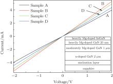
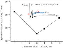
Figure 1 displays the results of room-temperature CTLM I − V measurement for four samples with different thicknesses of p+ + -InGaN layer when the spacing of the CTLM pattern is fixed at 30 μ m. As shown in Fig. 1, the CTLM I– V characteristics of the four samples show Ohmic contact behavior, and the current of Sample B is the largest one of these four samples. The measured current at 2.0 V between two metal pads with the gap spacing of 30 μ m is 5.4 mA for Sample B, but the corresponding currents are only 4.0 mA, 4.9 mA, and 4.6 mA, respectively for Samples A, C, and D. Figure 2 shows the specific contact resistivity (ρ c) as a function of the thickness of p+ + -InGaN layer. The ρ c values are both below 1.0× 10− 4 Ω · cm2 for Samples B and C, while the ρ c values for Samples A and D are much larger than the value of 1.0× 10− 4 Ω · cm2. Specifically, the lowest ρ c value obtained is 3.98× 10− 5 Ω · cm2 for Sample B.
In Sample A, the contact is made directly between metal and the heavily Mg-doped GaN, so the carrier transport is by variable-range hopping (VRH) conduction process through the DLD band.[15– 17] As previous reported, the transport mechanism of Ohmic contact using p+ + -InGaN contact layer attributes to enhanced tunneling effect.[12] The inset of Fig. 2 shows the schematic energy band diagrams of Ni/Au/p+ + -InGaN /p+ + -GaN/p-GaN contact at zero bias. The holes transport from the inner p-GaN layer to the interface between p+ + -GaN layer and p+ + -InGaN layer by VRH through DLD band, then they can directly tunnel across the p+ + -InGaN layer to the metal. The assistant effect of tunneling makes the carriers transportation easier, so when the thickness of p+ + -InGaN layer is in the range of 2 nm to 4 nm, low ρ c values below 1.0× 10− 4 Ω · cm2 can be obtained. The optimal thickness of p+ + -InGaN layer is 3 nm to form Ohmic contact. In Sample C, even though the p+ + -InGaN layer can also enhance the hole tunneling from p-GaN to metal Ni/Au, the InGaN layer is a little thicker, resulting in a lesser tunneling probability, so the value of ρ c is a little higher than that of Sample B. When the thickness of p+ + -InGaN layer increases to 6 nm in Sample D, it seems that the p+ + -InGaN layer is too thick to tunnel for the carriers, so the ρ c value of Sample D is much larger than that of Sample B.
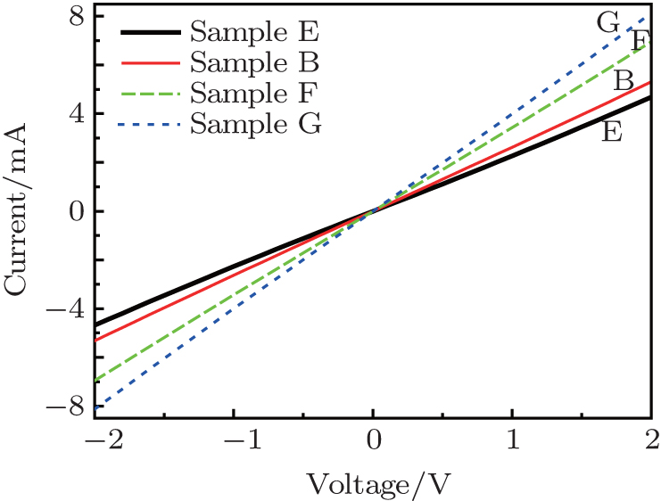
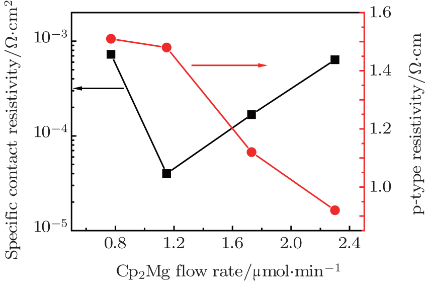
Figure 3 displays the results of CTLM I– V measurement for four samples with different Cp2Mg flow rates when the spacing of the CTLM pattern is fixed as 30 μ m at room temperature. As shown in Fig. 3, the current increases with the increase of Cp2Mg flow rate. Figure 4 shows the specific contact resistivity (ρ c) and p-type resistivity (ρ p) as a function of the Cp2Mg flow rate. It is seen that the specific contact resistivity (ρ c) decreases from 7.25× 10− 4 Ω · cm2 to 3.98× 10− 5 Ω · cm2 when the Cp2Mg flow rate increases from 0.77 μ mol/min to 1.15 μ mol/min firstly, and then increases to 6.37× 10− 4 Ω · cm2 when the Cp2Mg flow rate increases to 2.30 μ mol/min. It is interesting to note that the lowest ρ c value of 3.98× 10− 5 Ω · cm2 is obtained when the Cp2Mg flow rate of p+ + -InGaN layer is 1.15 μ mol/min, even though the current of CTLM I– V measurement is not the largest one. However, the p-type resistivity decreases from 1.51 Ω · cm to 0.92 Ω · cm when the Cp2Mg flow rate increases from 0.77 μ mol/min to 2.30 μ mol/min. This phenomenon may relate to the formation of 2DHG in the interface of InGaN/GaN heterojunction.
Due to the large piezoelectric polarization and large valance band discontinuity between GaN and InGaN, the surface of InGaN/GaN heterojunction shows a higher hole concentration above 1019 cm− 3, suggesting the formation of a 2DHG. A strong band bending is induced by 2DHG and strong polarization field. The formation of 2DHG needs p+ + -InGaN layer to be doped by adequate Mg to provide enough holes, so the value of ρ c increases to 7.25× 10− 4 Ω · cm2 when the Cp2Mg flow rate is only 0.77 μ mol/min for Sample E. Once the concentration of 2DHG is accumulated high enough at the interface between p+ + -GaN and p+ + -InGaN layer, the increasing Mg will affect the value of ρ p rather than ρ c. When the Cp2Mg flow rate increases from 1.15 to 2.30 μ mol/min, the decrease of ρ p resulting from the excessive 2DHG is larger than the increase of ρ c, resulting in the decrease of total resistance of CTLM measurement. So the current of CTLM measurement increases still, but the value of ρ c increases instead.
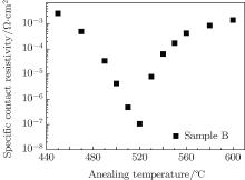
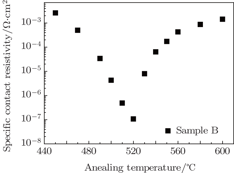
Figure 5 shows the ρ c values of sample B as a function of the alloying annealing temperature. As shown in Fig. 5, when the annealing temperature is between 490 ° C and 540 ° C, the ρ c value of sample B is less than 10− 4 Ω · cm2. The lowest ρ c of sample B is 1.07× 10− 7 Ω · cm2 after rapid thermal annealing at 520 ° C. This result indicates that the magnitude of ρ c is decreased by more than two orders through optimizing the alloying annealing temperature.
These results indicate that the suitable annealing temperature is important to achieve a low specific contact resistivity. As previously reported, the annealing temperature has a great effect on interfacial reaction between metal and semiconductors, or desorption of the nitrogen atoms from the p-type layer.[10, 18– 20] In addition, while it has not been clarified from the values of the thermal expansion coefficients for GaN and InGaN, the change of the strain at the two contact layers by changing the annealing temperature is also a possible reason for the increase in ρ c values. Further investigation is needed to clarify the mechanism of the effect of annealing temperature on the Ohmic contact performance using the p+ + -InGaN and p+ + -GaN compound contact layer. Based on these experimental results, the annealing temperature of 520 ° C is the best one for Ohmic contact. The compound contact layer whose growth conditions have been optimized greatly improves ohmic contact performance between the alloyed metal Ni/Au and p-GaN, that is to say, not only the magnitude of ρ c is decreased, but also the window of annealing temperature to get low specific contact resistivity is broadened to nearly 50 ° C.
4. SummaryIn summary, we have studied the dependence of Ohmic contact to p-GaN on the growth conditions of compound contact layer with different flow rate ratios between Mg and Ga gas sources and different thicknesses of p+ + -InGaN layer. The experimental results indicate that the performance of Ohmic contact with compound contact layer is better than that with only heavily Mg-doped GaN contact layer. The flow rate ratio between Mg and Ga gas sources of p+ + -InGaN layer has the optimal value, and too low or too high flow rate ratio will lead to the increase of specific contact resistivity. The thickness of p+ + -InGaN layer needs to be suitable to tunnel for carriers, so the thickness of 3 nm is the best for Ohmic contact to p-GaN. At last, the annealing temperature also has great effect on the performance of Ni/Au Ohmic contact to p-GaN. The optimal annealing temperature of 520 ° C results in the lowest specific contact resistivity of 1.07× 10− 7 Ω · cm2.


 , Jiang De-Sheng, Chen Ping, Zhu Jian-Jun, Liu Zong-Shun, Le Ling-Cong, Yang Jing, He Xiao-Guang]